SNAS207B May 2004 – January 2024 LM64
PRODUCTION DATA
- 1
- 1 Features
- 2 Applications
- 3 Description
- 4 Pin Configuration and Functions
- 5 Specifications
-
6 Detailed Description
- 6.1 Overview
- 6.2 Functional Block Diagram
- 6.3
Feature Description
- 6.3.1 Conversion Sequence
- 6.3.2 The ALERT Output
- 6.3.3 SMBus Interface
- 6.3.4 Power-On Reset (POR) Default States
- 6.3.5 Temperature Data Format
- 6.3.6 Open-Drain Outputs, Inputs, and Pull-Up Resistors
- 6.3.7 Diode Fault Detection
- 6.3.8 Communicating with the LM64
- 6.3.9 Digital Filter
- 6.3.10 Fault Queue
- 6.3.11 One-Shot Register
- 6.3.12 Serial Interface Reset
-
7 Registers
- 7.1
LM64 Registers
- 7.1.1 LM64 Register Map in Hexadecimal Order
- 7.1.2 LM64 Register Map in Functional Order
- 7.1.3 LM64 Initial Register Sequence and Register Descriptions in Functional Order
- 7.1.4
LM64 Register Descriptions in Functional Order
- 7.1.4.1 Fan Control Registers
- 7.1.4.2 Configuration Register
- 7.1.4.3 Tachometer Count And Limit Registers
- 7.1.4.4 Local Temperature And Local High Setpoint Registers
- 7.1.4.5 Remote Diode Temperature, Offset And Setpoint Registers
- 7.1.4.6 ALERT Status And Mask Registers
- 7.1.4.7 Conversion Rate And One-Shot Registers
- 7.1.4.8 ID Registers
- 7.2 General Purpose Registers
- 7.1
LM64 Registers
- 8 Application and Implementation
- 9 Layout
- 10Device and Documentation Support
- 11Revision History
- 12Mechanical, Packaging, and Orderable Information
Package Options
Mechanical Data (Package|Pins)
- NHW|24
Thermal pad, mechanical data (Package|Pins)
Orderable Information
8.1.3.1 Diode Non_Ideality
When a transistor is connected to a diode the following relationship holds for Vbe, T, and IF:
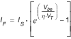
where

- q = 1.6x10⁻¹⁹ Coulombs (the electron charge)
- T = Absolute Temperature in Kelvin
- k = 1.38x10⁻²³ joules/K (Boltzmann’s constant)
- η is the non-ideality factor of the manufacturing process used to make the thermal diode
- Is = Saturation Current and is process dependent
- If = Forward Current through the base emitter junction
- Vbe = Base Emitter Voltage Drop
In the active region, the −1 term is negligible and may be eliminated, yielding the following equation

In the above equation, η and Is are dependent upon the process that was used in the fabrication of the particular diode. By forcing two currents with a very controlled ratio (N) and measuring the resulting voltage difference, it is possible to eliminate the Is term. Solving for the forward voltage difference yields the relationship:
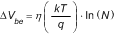
The non-ideality factor, η, is the only other parameter not accounted for and depends on the diode that is used for measurement. Since ΔVbe is proportional to both η and T, the variations in η cannot be distinguished from variations in temperature. Since the temperature sensor does not control the non-ideality factor, it will directly add to the inaccuracy of the sensor.
For example, if a processor manufacturer specifies a ±0.1% variation in η from part to part. As an example, assume that a temperature sensor has an accuracy specification of ±1°C at room temperature of 25°C. The resulting accuracy will be:
TACC = ±1°C + (±0.1% of 298°K) = ±1.3°C
The additional inaccuracy in the temperature measurement caused by η, can be eliminated if each temperature sensor is calibrated with the remote diode that it will be paired with. Refer to the processor datasheet for the non-ideality factor.