SNAS207B May 2004 – January 2024 LM64
PRODUCTION DATA
- 1
- 1 Features
- 2 Applications
- 3 Description
- 4 Pin Configuration and Functions
- 5 Specifications
-
6 Detailed Description
- 6.1 Overview
- 6.2 Functional Block Diagram
- 6.3
Feature Description
- 6.3.1 Conversion Sequence
- 6.3.2 The ALERT Output
- 6.3.3 SMBus Interface
- 6.3.4 Power-On Reset (POR) Default States
- 6.3.5 Temperature Data Format
- 6.3.6 Open-Drain Outputs, Inputs, and Pull-Up Resistors
- 6.3.7 Diode Fault Detection
- 6.3.8 Communicating with the LM64
- 6.3.9 Digital Filter
- 6.3.10 Fault Queue
- 6.3.11 One-Shot Register
- 6.3.12 Serial Interface Reset
-
7 Registers
- 7.1
LM64 Registers
- 7.1.1 LM64 Register Map in Hexadecimal Order
- 7.1.2 LM64 Register Map in Functional Order
- 7.1.3 LM64 Initial Register Sequence and Register Descriptions in Functional Order
- 7.1.4
LM64 Register Descriptions in Functional Order
- 7.1.4.1 Fan Control Registers
- 7.1.4.2 Configuration Register
- 7.1.4.3 Tachometer Count And Limit Registers
- 7.1.4.4 Local Temperature And Local High Setpoint Registers
- 7.1.4.5 Remote Diode Temperature, Offset And Setpoint Registers
- 7.1.4.6 ALERT Status And Mask Registers
- 7.1.4.7 Conversion Rate And One-Shot Registers
- 7.1.4.8 ID Registers
- 7.2 General Purpose Registers
- 7.1
LM64 Registers
- 8 Application and Implementation
- 9 Layout
- 10Device and Documentation Support
- 11Revision History
- 12Mechanical, Packaging, and Orderable Information
Package Options
Mechanical Data (Package|Pins)
- NHW|24
Thermal pad, mechanical data (Package|Pins)
Orderable Information
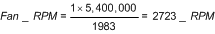
8.1.4 Computing RPM of the Fan from the TACH Count
The Tach Count Registers 46HEX and 47HEX count the number of periods of the 90 kHz tachometer clock in the LM64 for the tachometer input from the fan assuming a 2 pulse per revolution fan tachometer, such as the fans supplied with the Pentium 4 boxed processors. The RPM of the fan can be computed from the Tach Count Registers 46HEX and 47HEX. This can best be shown through an example.
Example:
Given: the fan used has a tachometer output with 2 per revolution.
Let:
Register 46 (LSB) is BFHEX = Decimal (11 x 16) + 15 = 191 and
Register 47 (MSB) is 7HEX = Decimal (7 x 256) = 1792.
The total Tach Count, in decimal, is 191 + 1792 = 1983.
The RPM is computed using the formula
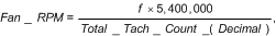
where
f = 1 for 2 pulses/rev fan tachometer output;
f = 2 for 1 pulse/rev fan tachometer output, and
f = 2 / 3 for 3 pulses/rev fan tachometer output
For our example