SNAS207B May 2004 – January 2024 LM64
PRODUCTION DATA
- 1
- 1 Features
- 2 Applications
- 3 Description
- 4 Pin Configuration and Functions
- 5 Specifications
-
6 Detailed Description
- 6.1 Overview
- 6.2 Functional Block Diagram
- 6.3
Feature Description
- 6.3.1 Conversion Sequence
- 6.3.2 The ALERT Output
- 6.3.3 SMBus Interface
- 6.3.4 Power-On Reset (POR) Default States
- 6.3.5 Temperature Data Format
- 6.3.6 Open-Drain Outputs, Inputs, and Pull-Up Resistors
- 6.3.7 Diode Fault Detection
- 6.3.8 Communicating with the LM64
- 6.3.9 Digital Filter
- 6.3.10 Fault Queue
- 6.3.11 One-Shot Register
- 6.3.12 Serial Interface Reset
-
7 Registers
- 7.1
LM64 Registers
- 7.1.1 LM64 Register Map in Hexadecimal Order
- 7.1.2 LM64 Register Map in Functional Order
- 7.1.3 LM64 Initial Register Sequence and Register Descriptions in Functional Order
- 7.1.4
LM64 Register Descriptions in Functional Order
- 7.1.4.1 Fan Control Registers
- 7.1.4.2 Configuration Register
- 7.1.4.3 Tachometer Count And Limit Registers
- 7.1.4.4 Local Temperature And Local High Setpoint Registers
- 7.1.4.5 Remote Diode Temperature, Offset And Setpoint Registers
- 7.1.4.6 ALERT Status And Mask Registers
- 7.1.4.7 Conversion Rate And One-Shot Registers
- 7.1.4.8 ID Registers
- 7.2 General Purpose Registers
- 7.1
LM64 Registers
- 8 Application and Implementation
- 9 Layout
- 10Device and Documentation Support
- 11Revision History
- 12Mechanical, Packaging, and Orderable Information
Package Options
Mechanical Data (Package|Pins)
- NHW|24
Thermal pad, mechanical data (Package|Pins)
Orderable Information
9.1 PCB Layout for Minimizing Noise
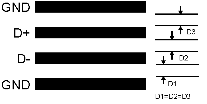
 Figure 9-1 Ideal Diode Trace Layout
In a noisy environment, such as a processor mother board, layout considerations are very critical. Noise induced on traces running between the remote temperature diode sensor and the LM64 can cause temperature conversion errors. Keep in mind that the signal level the LM64 is trying to measure is in microvolts. The following guidelines should be followed:
- Place a 0.1 µF power supply bypass capacitor as close as possible to the VDD pin and the recommended 2.2 nF capacitor as close as possible to the LM64's D+ and D− pins. Make sure the traces to the 2.2 nF capacitor are matched.
- Ideally, the LM64 should be placed within 10 cm of the Processor diode pins with the traces being as straight, short and identical as possible. Trace resistance of 1 Ω can cause as much as 1°C of error. This error can be compensated by using the Remote Temperature Offset Registers, since the value placed in these registers will automatically be subtracted from or added to the remote temperature reading.
- Diode traces should be surrounded by a GND guard ring to either side, above and below if possible. This GND guard should not be between the D+ and D− lines. In the event that noise does couple to the diode lines it would be ideal if it is coupled common mode. That is equally to the D+ and D− lines.
- Avoid routing diode traces in close proximity to power supply switching or filtering inductors.
- Avoid running diode traces close to or parallel to high speed digital and bus lines. Diode traces should be kept at least 2 cm apart from the high speed digital traces.
- If it is necessary to cross high speed digital traces, the diode traces and the high speed digital traces should cross at a 90 degree angle.
- The ideal place to connect the LM64's GND pin is as close as possible to the Processor's GND associated with the sense diode.
- Leakage current between D+ and GND should be kept to a minimum. One nano-ampere of leakage can cause as much as 1°C of error in the diode temperature reading. Keeping the printed circuit board as clean as possible will minimize leakage current.
Noise coupling into the digital lines greater than 400 mVp-p (typical hysteresis) and undershoot less than 500 mV below GND, may prevent successful SMBus communication with the LM64. SMBus no acknowledge is the most common symptom, causing unnecessary traffic on the bus. Although the SMBus maximum frequency of communication is rather low (100 kHz max), care still needs to be taken to ensure proper termination within a system with multiple parts on the bus and long printed circuit board traces. An RC lowpass filter with a 3 dB corner frequency of about 40 MHz is included on the LM64's SMBCLK input. Additional resistance can be added in series with the SMBData and SMBCLK lines to further help filter noise and ringing. Minimize noise coupling by keeping digital traces out of switching power supply areas as well as ensuring that digital lines containing high speed data communications cross at right angles to the SMBData and SMBCLK lines.