SNAS207B May 2004 – January 2024 LM64
PRODUCTION DATA
- 1
- 1 Features
- 2 Applications
- 3 Description
- 4 Pin Configuration and Functions
- 5 Specifications
-
6 Detailed Description
- 6.1 Overview
- 6.2 Functional Block Diagram
- 6.3
Feature Description
- 6.3.1 Conversion Sequence
- 6.3.2 The ALERT Output
- 6.3.3 SMBus Interface
- 6.3.4 Power-On Reset (POR) Default States
- 6.3.5 Temperature Data Format
- 6.3.6 Open-Drain Outputs, Inputs, and Pull-Up Resistors
- 6.3.7 Diode Fault Detection
- 6.3.8 Communicating with the LM64
- 6.3.9 Digital Filter
- 6.3.10 Fault Queue
- 6.3.11 One-Shot Register
- 6.3.12 Serial Interface Reset
-
7 Registers
- 7.1
LM64 Registers
- 7.1.1 LM64 Register Map in Hexadecimal Order
- 7.1.2 LM64 Register Map in Functional Order
- 7.1.3 LM64 Initial Register Sequence and Register Descriptions in Functional Order
- 7.1.4
LM64 Register Descriptions in Functional Order
- 7.1.4.1 Fan Control Registers
- 7.1.4.2 Configuration Register
- 7.1.4.3 Tachometer Count And Limit Registers
- 7.1.4.4 Local Temperature And Local High Setpoint Registers
- 7.1.4.5 Remote Diode Temperature, Offset And Setpoint Registers
- 7.1.4.6 ALERT Status And Mask Registers
- 7.1.4.7 Conversion Rate And One-Shot Registers
- 7.1.4.8 ID Registers
- 7.2 General Purpose Registers
- 7.1
LM64 Registers
- 8 Application and Implementation
- 9 Layout
- 10Device and Documentation Support
- 11Revision History
- 12Mechanical, Packaging, and Orderable Information
Package Options
Mechanical Data (Package|Pins)
- NHW|24
Thermal pad, mechanical data (Package|Pins)
Orderable Information
5.8 SMBus Digital Switching Characteristics
Unless otherwise noted, these specifications apply for VDD = +3.0 VDC to +3.6 VDC, CL (load capacitance) on output lines = 80 pF. Boldface limits apply for TA = TJ; TMIN ≤ TA ≤ TMAX; all other limits TA = TJ = +25°C, unless otherwise noted. The switching characteristics of the LM64 fully meet or exceed the published specifications of the SMBus version 2.0. The following parameters are the timing relationships between SMBCLK and SMBDAT signals related to the LM64. They adhere to but are not necessarily the same as the SMBus bus specifications.
| Symbol | Parameter | Conditions | Limits (1) | Units (Limit) |
|---|---|---|---|---|
| fSMB | SMBus Clock Frequency | 10 100 | kHz (min) kHz (max) | |
| tLOW | SMBus Clock Low Time | From VIN(0) max to VIN(0) max | 4.7 | µs (min) |
| tHIGH | SMBus Clock High Time | From VIN(1) min to VIN(1) min | 4.0 50 | µs (min) µs (max) |
| tR | SMBus Rise Time | See (2) | 1 | µs (max) |
| tF | SMBus Fall Time | See (3) | 0.3 | µs (max) |
| tOF | Output Fall Time | CL = 400 pF, IO = 3 mA | 250 | ns (max) |
| tTIMEOUT | SMBData and SMBCLK Time Low for Reset of Serial Interface See (4) | 25 35 | ms (min) ms (max) | |
| tSU:DAT | Data In Setup Time to SMBCLK High | 250 | ns (min) | |
| tHD:DAT | Data Out Hold Time after SMBCLK Low | 300 930 | ns (min) ns (max) | |
| tHD:STA | Hold Time after (Repeated) Start Condition. After this period the first clock is generated. | 4.0 | µs (min) | |
| tSU:STO | Stop Condition SMBCLK High to SMBDAT Low (Stop Condition Setup) | 100 | ns (min) | |
| tSU:STA | SMBus Repeated Start-Condition Setup Time, SMBCLK High to SMBDAT Low | 4.7 | µs (min) | |
| tBUF | SMBus Free Time between Stop and Start Conditions | 4.7 | µs (min) |
(1) Limits are guaranteed to TI's AOQL (Average Outgoing Quality Level).
(2) The output rise time is measured from (VIL max - 0.15 V) to (VIH min + 0.15 V).
(3) The output fall time is measured from (VIH min + 0.15 V) to (VIL min - 0.15 V).
(4) Holding the SMBData and/or SMBCLK lines Low for a time interval greater than tTIMEOUT will reset the LM64’s SMBus state machine, therefore setting SMBDAT and SMBCLK pins to a high impedance state.
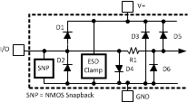
 Figure 5-1 SMBus Timing Diagram for SMBCLK and SMBDAT Signals
Table 5-1
| Pin Name | Pin # | D1 | D2 | D3 | D4 | D5 | D6 | R1 | SNP | ESD CLAMP |
|---|---|---|---|---|---|---|---|---|---|---|
| GPIO1 | 1 | X | X | X | ||||||
| GPIO2 | 2 | X | X | X | ||||||
| GPIO3 | 3 | X | X | X | ||||||
| PWM | 4 | X | X | X | ||||||
| VDD | 5 | X | ||||||||
| D+ | 6 | X | X | X | X | X | X | |||
| D− | 7 | X | X | X | X | X | X | |||
| T_Crit | 8 | X | X | X | X | |||||
| A0 | 12 | X | ||||||||
| ALERT | 14 | X | X | X | X | |||||
| TACH | 15 | X | X | X | ||||||
| SMBDAT | 16 | X | X | X | ||||||
| SMBCLK | 17 | X | ||||||||
| GPIO5 | 18 | X | X | X | ||||||
| GPIO4 | 19 | X | X | X | ||||||
| GPD1 | 20 | X | ||||||||
| GPD2 | 21 | X | ||||||||
| GPD3 | 22 | X | ||||||||
| GPD4 | 23 | X | ||||||||
| GPD5 | 24 | X |
 Figure 5-2 ESD Protection Input Structure