SNVSBW0B October 2022 – August 2024 LM64440-Q1 , LM64460-Q1
PRODUCTION DATA
- 1
- 1 Features
- 2 Applications
- 3 Description
- 4 Device Comparison Table
- 5 Pin Configuration and Functions
- 6 Specifications
-
7 Detailed Description
- 7.1 Overview
- 7.2 Functional Block Diagram
- 7.3
Feature Description
- 7.3.1 Input Voltage Range (VIN1, VIN2)
- 7.3.2 Output Voltage Setpoint (FB)
- 7.3.3 Precision Enable and Input Voltage UVLO (EN)
- 7.3.4 MODE/SYNC Operation
- 7.3.5 Clock Locking
- 7.3.6 Power-Good Monitor (PGOOD)
- 7.3.7 Bias Supply Regulator (VCC, BIAS)
- 7.3.8 Bootstrap Voltage and UVLO (CBOOT)
- 7.3.9 Spread Spectrum
- 7.3.10 Soft Start and Recovery From Dropout
- 7.3.11 Overcurrent and Short-Circuit Protection
- 7.3.12 Thermal Shutdown
- 7.3.13 Input Supply Current
- 7.4 Device Functional Modes
-
8 Application and Implementation
- 8.1 Application Information
- 8.2
Typical Applications
- 8.2.1 Design 1 – Automotive Synchronous 6A Buck Regulator at 2.1MHz
- 8.2.2
Design 2 – Automotive Synchronous 4A Buck Regulator at 2.1MHz
- 8.2.2.1 Design Requirements
- 8.2.2.2
Detailed Design Procedure
- 8.2.2.2.1 Custom Design With WEBENCH® Tools
- 8.2.2.2.2 Setting the Output Voltage
- 8.2.2.2.3 Choosing the Switching Frequency
- 8.2.2.2.4 Inductor Selection
- 8.2.2.2.5 Output Capacitor Selection
- 8.2.2.2.6 Input Capacitor Selection
- 8.2.2.2.7 Bootstrap Capacitor
- 8.2.2.2.8 VCC Capacitor
- 8.2.2.2.9 BIAS Power Connection
- 8.2.2.2.10 Feedforward Network
- 8.2.2.2.11 Input Voltage UVLO
- 8.2.2.3 Application Curves
- 8.3 Power Supply Recommendations
- 8.4 Layout
- 9 Device and Documentation Support
- 10Revision History
- 11Mechanical, Packaging, and Orderable Information
Package Options
Mechanical Data (Package|Pins)
- RYF|22
Thermal pad, mechanical data (Package|Pins)
Orderable Information
7.3.6 Power-Good Monitor (PGOOD)
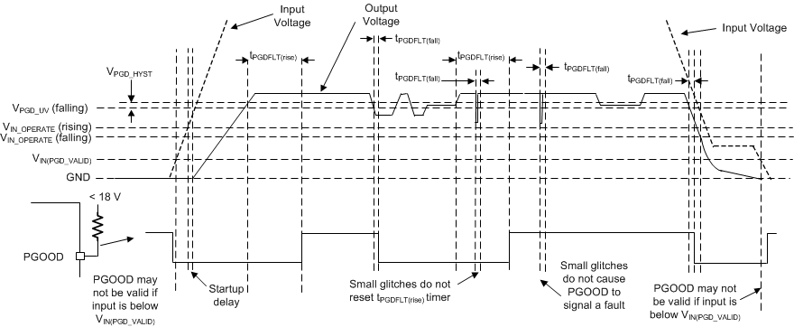
The PGOOD function is implemented to replace a discrete reset device, reducing BOM count and cost. The PGOOD voltage goes low when the feedback (FB) voltage is outside of the specified PGOOD thresholds (see Figure 6-8). This can occur during current limit and thermal shutdown, as well as when disabled and during normal start-up. A glitch filter prevents false flag operation for short excursions of the output voltage, such as during line and load transients. Output voltage excursions that are shorter than tPGDFLT(fall) do not trip the PGOOD flag. Refer to Figure 7-13 to best understand PGOOD operation.
The PGOOD output consists of an open-drain N-channel transistor, requiring an external pullup resistor to a suitable logic supply or VOUT. When EN is pulled low, the flag output is also forced low. With EN low, PGOOD remains valid as long as the input voltage is above 1V (typical).
 Figure 7-13 PGOOD Timing Diagram (Excludes OV Events)
| FAULT CONDITION INITIATED | FAULT CONDITION ENDS (AFTER WHICH tPGDFLT(rise) MUST PASS BEFORE PGOOD OUTPUT IS RELEASED)(1) |
|---|---|
| VOUT < VOUT-target × PGDUV AND t > tPGDFLT(fall) | Output voltage in regulation: VOUT-target × (PGDUV + PGDHYST) < VOUT < VOUT-target × (PGDOV – PGDHYST) (see Figure 6-8) |
| VOUT > VOUT-target × PGDOV AND t > tPGDFLT(fall) | Output voltage in regulation |
| TJ > TSHD | TJ < TSHD-F AND output voltage in regulation |
| VEN < VEN-TH falling | VEN > VEN-TH rising AND output voltage in regulation |
| VCC < VCC-UVLO - VCC-UVLO-HYST | VCC > VCC-UVLO AND output voltage in regulation |