SNVSCW3 November 2024 LM644A2-Q1
PRODUCTION DATA
- 1
- 1 Features
- 2 Applications
- 3 Description
- 4 Device Comparison Table
- 5 Pin Configuration and Functions
- 6 Specifications
-
7 Detailed Description
- 7.1 Overview
- 7.2 Functional Block Diagram
- 7.3
Feature Description
- 7.3.1 Input Voltage Range (VIN)
- 7.3.2 Enable EN Pin and Use as VIN UVLO
- 7.3.3 Output Voltage Selection and Soft Start
- 7.3.4 SYNC Allows Clock Synchronization and Mode Selection
- 7.3.5 Clock Locking
- 7.3.6 Adjustable Switching Frequency
- 7.3.7 Power-Good Output Voltage Monitoring
- 7.3.8 Internal LDO, VCC UVLO, and BIAS Input
- 7.3.9 Bootstrap Voltage and VCBOOT-UVLO (CB1 and CB2 Pin)
- 7.3.10 CONFIG Device Configuration Pin
- 7.3.11 Spread Spectrum
- 7.3.12 Soft Start and Recovery From Dropout
- 7.3.13 Overcurrent and Short-Circuit Protection
- 7.3.14 Hiccup
- 7.3.15 Thermal Shutdown
- 7.4 Device Functional Modes
-
8 Application and Implementation
- 8.1 Application Information
- 8.2
Typical Application
- 8.2.1 Design Requirements
- 8.2.2
Detailed Design Procedure
- 8.2.2.1 Choosing the Switching Frequency
- 8.2.2.2 Setting the Output Voltage
- 8.2.2.3 Inductor Selection
- 8.2.2.4 Output Capacitor Selection
- 8.2.2.5 Input Capacitor Selection
- 8.2.2.6 BOOT Capacitor
- 8.2.2.7 VCC
- 8.2.2.8 CFF and RFF Selection
- 8.2.2.9 SYNCHRONIZATION AND MODE
- 8.2.2.10 External UVLO
- 8.2.2.11 Typical Thermal Performance
- 8.2.3 Application Curves
- 8.3 Power Supply Recommendations
- 8.4 Layout
- 9 Device and Documentation Support
- 10Revision History
- 11Mechanical, Packaging, and Orderable Information
Package Options
Mechanical Data (Package|Pins)
- VBG|24
Thermal pad, mechanical data (Package|Pins)
Orderable Information
7.4.3.2.1 Diode Emulation
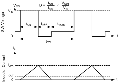
Diode emulation prevents reverse current though the inductor, which requires a lower frequency needed to regulate given a fixed peak inductor current. Diode emulation also limits ripple current as frequency is reduced. Frequency is reduced when peak inductor current goes below IPEAK-MIN. With a fixed peak current, as output current is reduced to zero, frequency must be reduced to near zero to maintain regulation.

The LM644A2-Q1 has a minimum peak inductor current setting in auto mode. That being said, when current is reduced to a low value with fixed input voltage, on-time is constant. Regulation is then achieved by adjusting frequency . This mode of operation is called PFM mode regulation.