SNVSCW3 November 2024 LM644A2-Q1
PRODUCTION DATA
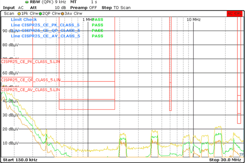
- 1
- 1 Features
- 2 Applications
- 3 Description
- 4 Device Comparison Table
- 5 Pin Configuration and Functions
- 6 Specifications
-
7 Detailed Description
- 7.1 Overview
- 7.2 Functional Block Diagram
- 7.3
Feature Description
- 7.3.1 Input Voltage Range (VIN)
- 7.3.2 Enable EN Pin and Use as VIN UVLO
- 7.3.3 Output Voltage Selection and Soft Start
- 7.3.4 SYNC Allows Clock Synchronization and Mode Selection
- 7.3.5 Clock Locking
- 7.3.6 Adjustable Switching Frequency
- 7.3.7 Power-Good Output Voltage Monitoring
- 7.3.8 Internal LDO, VCC UVLO, and BIAS Input
- 7.3.9 Bootstrap Voltage and VCBOOT-UVLO (CB1 and CB2 Pin)
- 7.3.10 CONFIG Device Configuration Pin
- 7.3.11 Spread Spectrum
- 7.3.12 Soft Start and Recovery From Dropout
- 7.3.13 Overcurrent and Short-Circuit Protection
- 7.3.14 Hiccup
- 7.3.15 Thermal Shutdown
- 7.4 Device Functional Modes
-
8 Application and Implementation
- 8.1 Application Information
- 8.2
Typical Application
- 8.2.1 Design Requirements
- 8.2.2
Detailed Design Procedure
- 8.2.2.1 Choosing the Switching Frequency
- 8.2.2.2 Setting the Output Voltage
- 8.2.2.3 Inductor Selection
- 8.2.2.4 Output Capacitor Selection
- 8.2.2.5 Input Capacitor Selection
- 8.2.2.6 BOOT Capacitor
- 8.2.2.7 VCC
- 8.2.2.8 CFF and RFF Selection
- 8.2.2.9 SYNCHRONIZATION AND MODE
- 8.2.2.10 External UVLO
- 8.2.2.11 Typical Thermal Performance
- 8.2.3 Application Curves
- 8.3 Power Supply Recommendations
- 8.4 Layout
- 9 Device and Documentation Support
- 10Revision History
- 11Mechanical, Packaging, and Orderable Information
Package Options
Mechanical Data (Package|Pins)
- VBG|24
Thermal pad, mechanical data (Package|Pins)
Orderable Information
3 Description
The LM644A2-Q1 is a 36V, synchronous, buck, DC/DC converter for high-current single or dual outputs. The device uses an interleaved, stackable, current-mode control architecture for easy loop compensation, fast transient response, excellent load and line regulation, and accurate current sharing with an output clock supporting up to 6 phases for currents up to 36A. A high-side switch minimum on-time of 50ns gives large step-down ratios, enabling the direct conversion from 12V, 24V, or automotive inputs to low-voltage rails for reduced system complexity and design cost.
The LM644A2-Q1 incorporates spread spectrum in an optimized enhanced HotRod QFN package, with wettable flanks, and low inductance input bypass configuration to minimize EMI. Dual Random Spread Spectrum (DRSS) frequency hopping is set to ±10% (typical), drastically reducing emissions through a combination of triangular and pseudo-random modulation. A bias pin allows the LM644A2-Q1 to save losses by powering the device from the output of the converter, achieving a 9μA no-load quiescent current to extend the operating run-time in battery-powered systems. The LM644A2-Q1 can maintain high efficiency light-load operation even when stacking multiple devices for high efficiency over the full load range.
| PART NUMBER | PACKAGE(1) | PACKAGE SIZE(2) |
|---|---|---|
| LM644A2-Q1 | VBG (WQFN-FCRLF, 24) | 5mm × 4mm |
 CISPR 25
Conducted, VOUT = 3.3V, 2.1MHz, 12A