SLVSGD6A November 2021 – March 2022 LM66100-Q1
PRODUCTION DATA
- 1 Features
- 2 Applications
- 3 Description
- 4 Revision History
- 5 Pin Configuration and Functions
- 6 Specifications
- 7 Parameter Measurement Information
- 8 Detailed Description
- 9 Application and Implementation
- 10Power Supply Recommendations
- 11Layout
- 12Device and Documentation Support
- 13Mechanical, Packaging, and Orderable Information
Package Options
Mechanical Data (Package|Pins)
- DCK|6
Thermal pad, mechanical data (Package|Pins)
Orderable Information
5 Pin Configuration and Functions
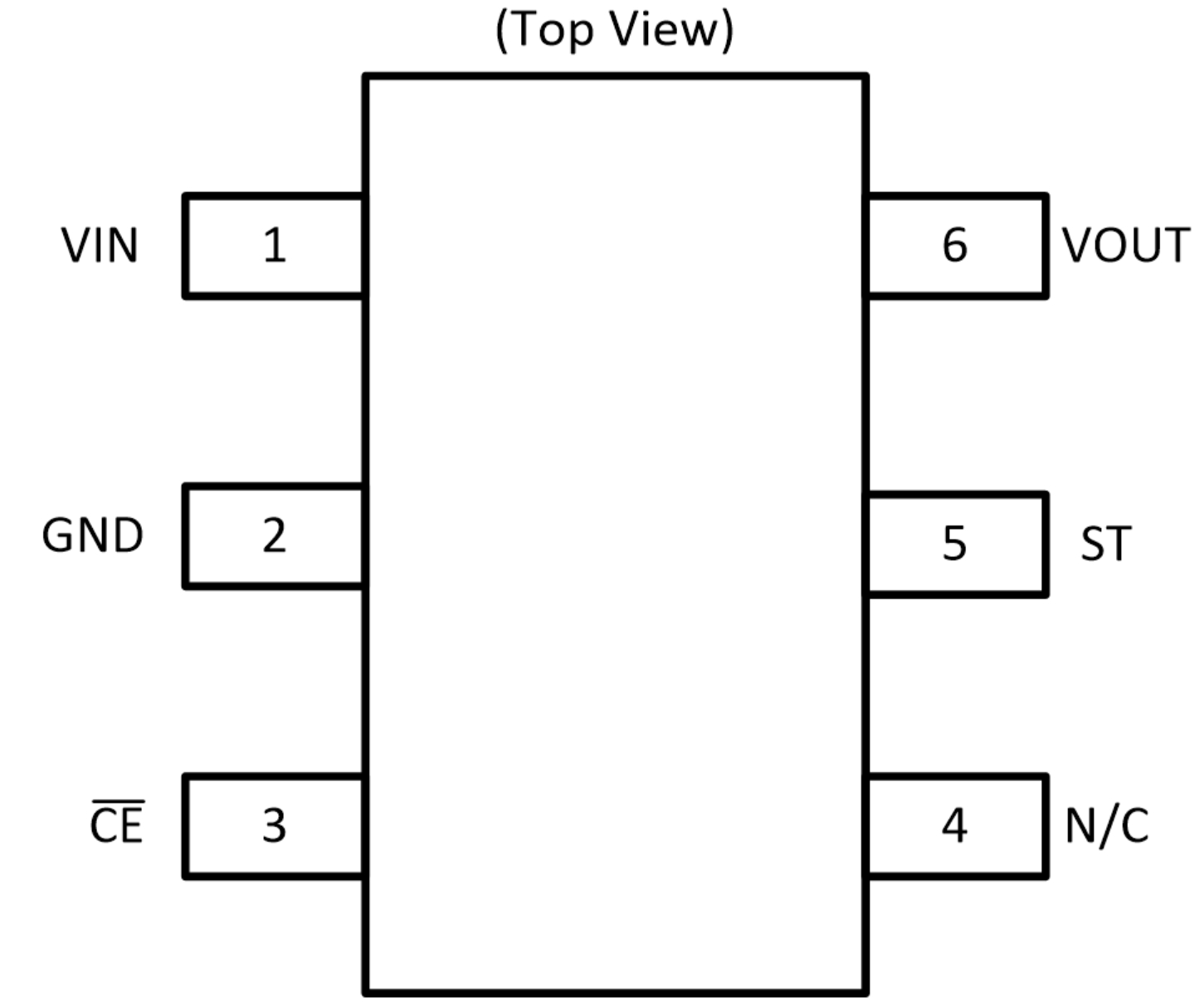
 Figure 5-1 DCK Package6-Pin SC-70Top View
Table 5-1 Pin Functions
| PIN | I/O | DESCRIPTION | |
|---|---|---|---|
| NO. | NAME | ||
| 1 | VIN | I | Device input |
| 2 | GND | — | Device ground |
| 3 | CE | I | Active-low chip enable. Can be connected to VOUT for reverse current protection. Do not leave floating. |
| 4 | N/C | — | Not internally connected, can be tied to GND or left floating. |
| 5 | ST | O | Active-low open-drain output, pulled low when the chip is disabled. Hi-Z when the chip is enabled. Connect to GND if not required. |
| 6 | VOUT | O | Device output |