SLVSG04
November 2021
LM66200
PRODUCTION DATA
1
Features
2
Applications
3
Description
4
Revision History
5
Pin Configuration and Functions
6
Specifications
6.1
Absolute Maximum Ratings
6.2
ESD Ratings
6.3
Recommended Operating Conditions
6.4
Thermal Information
6.5
Electrical Characteristics
6.6
Switching Characteristics
6.7
Typical Characteristics
7
Detailed Description
7.1
Overview
7.2
Functional Block Diagram
7.3
Feature Description
7.3.1
Truth Table
7.3.2
Soft Start
7.3.3
Status Indication
7.4
VINx Collapse Rate
7.5
Output Voltage Drop
7.6
Device Functional Modes
7.6.1
Automatic Switchover
8
Application and Implementation
8.1
Application Information
8.2
Typical Application
8.2.1
Design Requirements
8.2.2
Detailed Design Procedure
8.2.3
Application Performance Plots
9
Power Supply Recommendations
10
Layout
10.1
Layout Guidelines
10.2
Layout Example
11
Device and Documentation Support
11.1
Documentation Support
11.1.1
Related Documentation
11.2
Receiving Notification of Documentation Updates
11.3
Trademarks
11.4
Electrostatic Discharge Caution
11.5
Glossary
12
Mechanical, Packaging, and Orderable Information
Package Options
Mechanical Data (Package|Pins)
DRL|8
MPCS002E
Thermal pad, mechanical data (Package|Pins)
Orderable Information
slvsg04_oa
slvsg04_pm
6.7
Typical Characteristics
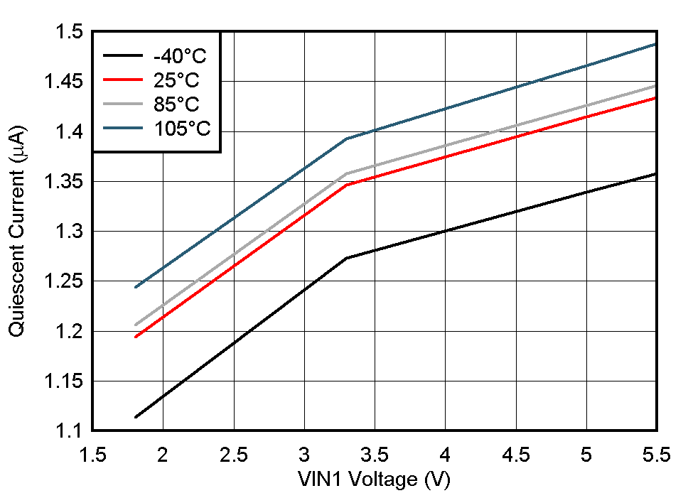
VIN2 = 1.6 V
VOUT = Open
Figure 6-1
VIN1 Quiescent Current vs Input Voltage
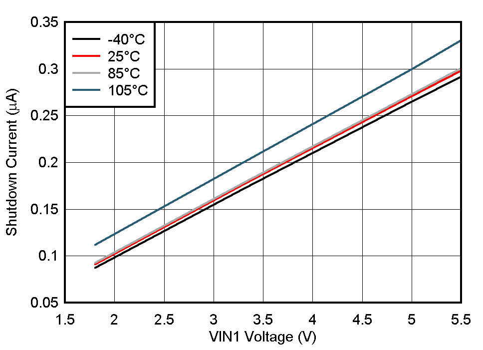
VIN2 = 1.6 V
VOUT = 0 V
Figure 6-3
VIN1 Shutdown Current vs Input Voltage
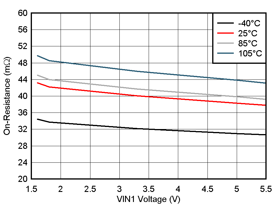
I
OUT
= 200 mA
Figure 6-5
Channel 1 On-Resistance vs Input Voltage
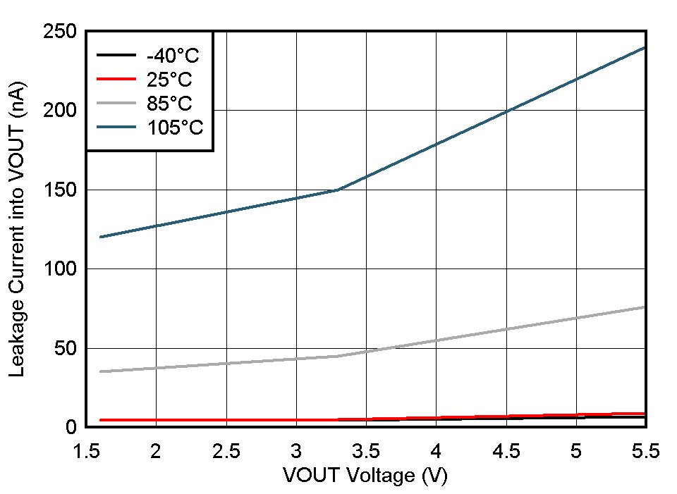
V
INx
= 0 V
V
INy
= Open
Figure 6-7
Reverse Leakage Current into VOUT
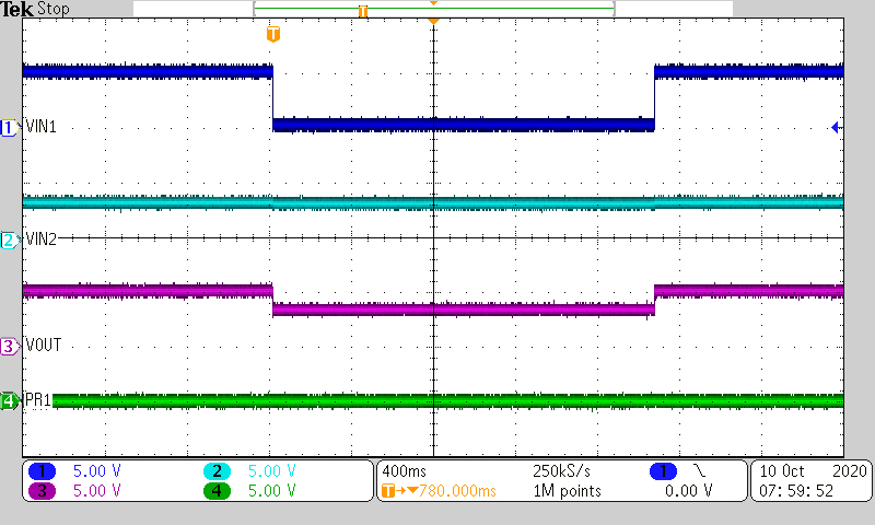
Figure 6-9
Diode Mode Switchover Behavior (R
L
= 10 Ω, CL = 10 uF)
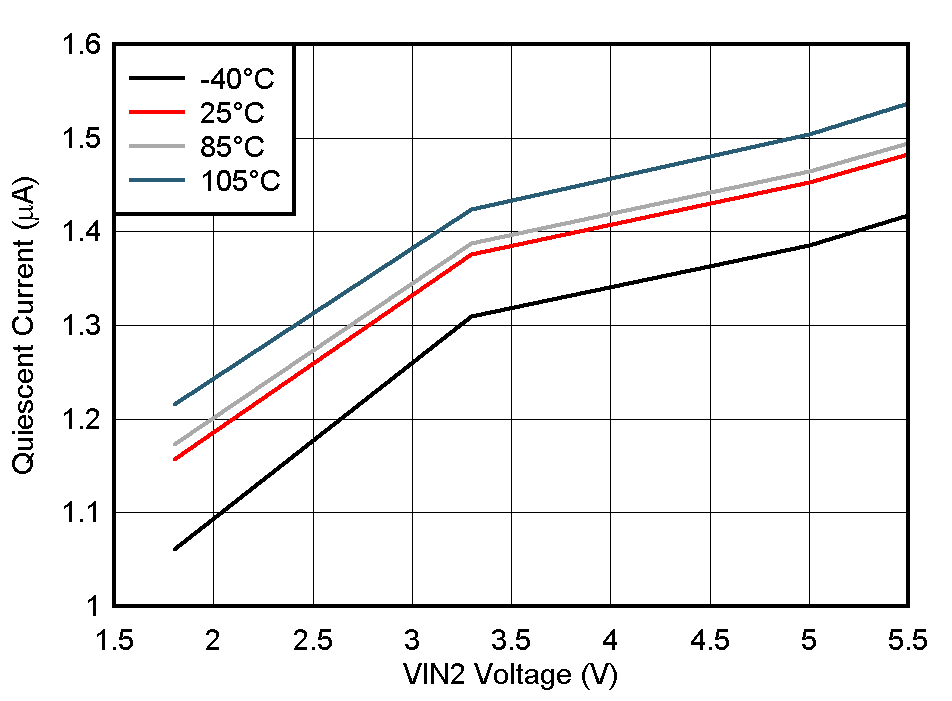
VIN1 = 1.6 V
VOUT = Open
Figure 6-2
VIN2 Quiescent Current vs Input Voltage
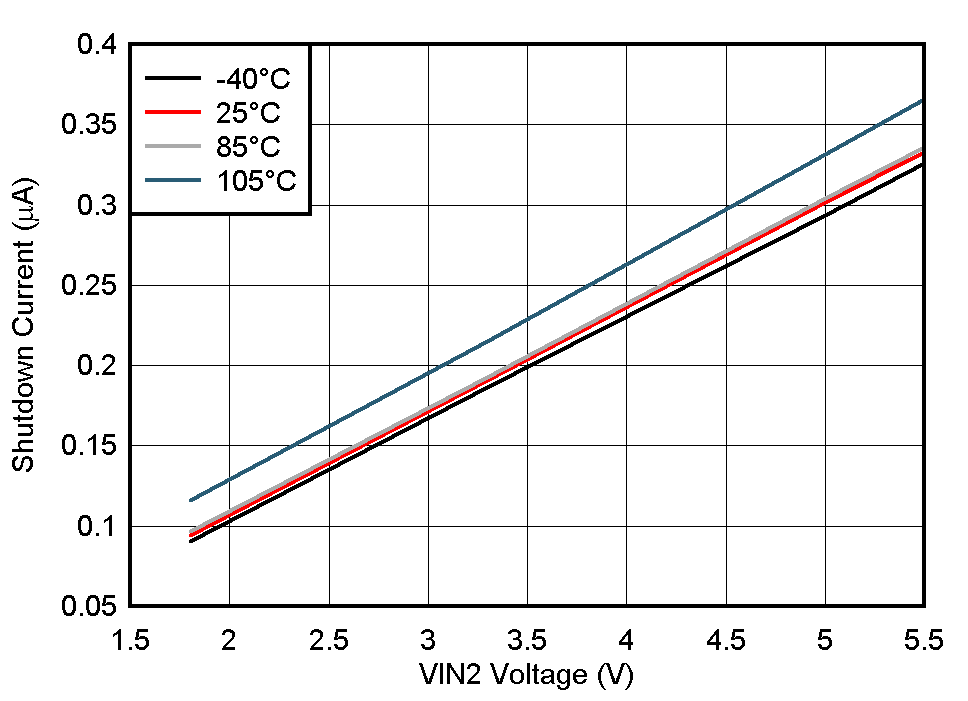
VIN1 = 1.6 V
VOUT = 0 V
Figure 6-4
VIN2 Shutdown Current vs Input Voltage
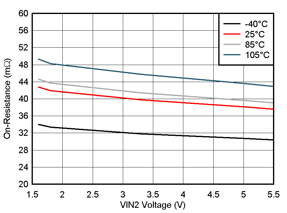
I
OUT
= 200 mA
Figure 6-6
Channel 2 On-Resistance vs Input Voltage
V
INx
= 0 V
V
INy
= Open
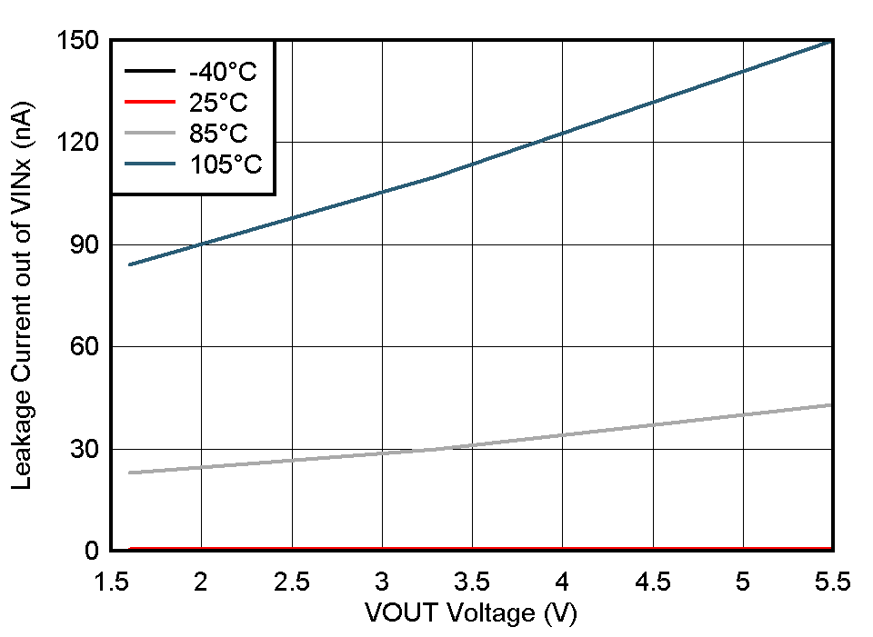
Figure 6-8
Reverse Leakage Current out of VINx