SNVSBX7A September 2023 – June 2024 LM70840-Q1 , LM70860-Q1 , LM70880-Q1
PRODUCTION DATA
- 1
- 1 Features
- 2 Applications
- 3 Description
- 4 Description (continued)
- 5 Pin Configuration and Functions
- 6 Specifications
-
7 Detailed Description
- 7.1 Overview
- 7.2 Functional Block Diagram
- 7.3
Feature Description
- 7.3.1 Input Voltage Range (VIN)
- 7.3.2 High-Voltage Bias Supply Regulator (VCC, BIAS, VDDA)
- 7.3.3 Enable (EN)
- 7.3.4 Power-Good Monitor (PG)
- 7.3.5 Switching Frequency (RT)
- 7.3.6 Dual Random Spread Spectrum (DRSS)
- 7.3.7 Soft Start
- 7.3.8 Output Voltage Setpoint (FB)
- 7.3.9 Minimum Controllable On-Time
- 7.3.10 Error Amplifier and PWM Comparator (FB, EXTCOMP)
- 7.3.11 Slope Compensation
- 7.3.12 Shunt Current Sensing
- 7.3.13 Hiccup Mode Current Limiting
- 7.3.14 Device Configuration (CONFIG)
- 7.3.15 Single-Output Dual-phase Operation
- 7.3.16 Pulse Frequency Modulation (PFM) / Synchronization
- 7.3.17 Thermal Shutdown (TSD)
- 7.4 Device Functional Modes
-
8 Application and Implementation
- 8.1 Application Information
- 8.2
Typical Applications
- 8.2.1
Design 1 – High Efficiency, Wide Input, 400-kHz Synchronous
Buck Regulator
- 8.2.1.1 Design Requirements
- 8.2.1.2
Detailed Design Procedure
- 8.2.1.2.1 Custom Design With WEBENCH® Tools
- 8.2.1.2.2 Custom Design With Excel Quickstart Tool
- 8.2.1.2.3 Buck Inductor
- 8.2.1.2.4 Current-Sense Resistance
- 8.2.1.2.5 Output Capacitors
- 8.2.1.2.6 Input Capacitors
- 8.2.1.2.7 Frequency Set Resistor
- 8.2.1.2.8 Feedback Resistors
- 8.2.1.2.9 Compensation Components
- 8.2.1.3 Application Curves
- 8.2.2 Design 2 – High Efficiency 48V to 12V 400kHz Synchronous Buck Regulator
- 8.2.1
Design 1 – High Efficiency, Wide Input, 400-kHz Synchronous
Buck Regulator
- 8.3 Power Supply Recommendations
- 8.4 Layout
- 9 Device and Documentation Support
- 10Revision History
- 11Mechanical, Packaging, and Orderable Information
Package Options
Mechanical Data (Package|Pins)
- RRX|29
Thermal pad, mechanical data (Package|Pins)
Orderable Information
8.1.2 Error Amplifier and Compensation
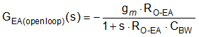
A Type-ll compensator using a transconductance error amplifier (EA) is shown in Figure 8-3. The dominant pole of the EA open-loop gain is set by the EA output resistance, ROEA, and effective bandwidth-limiting capacitance, CBW as shown by Equation 23.
The EA high-frequency pole is neglected in the above expression. The compensator transfer function from output voltage to COMP node, including the gain contribution from the (internal or external) feedback resistor network, is calculated in Equation 25.
where
- VREF is the feedback voltage reference of 0.8V
- gm is the EA gain transconductance of 1200µS
- RO-EA is the error amplifier output impedance of 64MΩ
The EA compensation components create a pole close to the origin, a zero, and a high-frequency pole. Typically, RCOMP << RO-EA and CCOMP >> CBW and CHF, so the approximations are valid.Figure 8-3 circles the poles in red and the zero in blue.
 Figure 8-3 Error
Amplifier and Compensation Network
Figure 8-3 Error
Amplifier and Compensation Network