SNVSBX7A September 2023 – June 2024 LM70840-Q1 , LM70860-Q1 , LM70880-Q1
PRODUCTION DATA
- 1
- 1 Features
- 2 Applications
- 3 Description
- 4 Description (continued)
- 5 Pin Configuration and Functions
- 6 Specifications
-
7 Detailed Description
- 7.1 Overview
- 7.2 Functional Block Diagram
- 7.3
Feature Description
- 7.3.1 Input Voltage Range (VIN)
- 7.3.2 High-Voltage Bias Supply Regulator (VCC, BIAS, VDDA)
- 7.3.3 Enable (EN)
- 7.3.4 Power-Good Monitor (PG)
- 7.3.5 Switching Frequency (RT)
- 7.3.6 Dual Random Spread Spectrum (DRSS)
- 7.3.7 Soft Start
- 7.3.8 Output Voltage Setpoint (FB)
- 7.3.9 Minimum Controllable On-Time
- 7.3.10 Error Amplifier and PWM Comparator (FB, EXTCOMP)
- 7.3.11 Slope Compensation
- 7.3.12 Shunt Current Sensing
- 7.3.13 Hiccup Mode Current Limiting
- 7.3.14 Device Configuration (CONFIG)
- 7.3.15 Single-Output Dual-phase Operation
- 7.3.16 Pulse Frequency Modulation (PFM) / Synchronization
- 7.3.17 Thermal Shutdown (TSD)
- 7.4 Device Functional Modes
-
8 Application and Implementation
- 8.1 Application Information
- 8.2
Typical Applications
- 8.2.1
Design 1 – High Efficiency, Wide Input, 400-kHz Synchronous
Buck Regulator
- 8.2.1.1 Design Requirements
- 8.2.1.2
Detailed Design Procedure
- 8.2.1.2.1 Custom Design With WEBENCH® Tools
- 8.2.1.2.2 Custom Design With Excel Quickstart Tool
- 8.2.1.2.3 Buck Inductor
- 8.2.1.2.4 Current-Sense Resistance
- 8.2.1.2.5 Output Capacitors
- 8.2.1.2.6 Input Capacitors
- 8.2.1.2.7 Frequency Set Resistor
- 8.2.1.2.8 Feedback Resistors
- 8.2.1.2.9 Compensation Components
- 8.2.1.3 Application Curves
- 8.2.2 Design 2 – High Efficiency 48V to 12V 400kHz Synchronous Buck Regulator
- 8.2.1
Design 1 – High Efficiency, Wide Input, 400-kHz Synchronous
Buck Regulator
- 8.3 Power Supply Recommendations
- 8.4 Layout
- 9 Device and Documentation Support
- 10Revision History
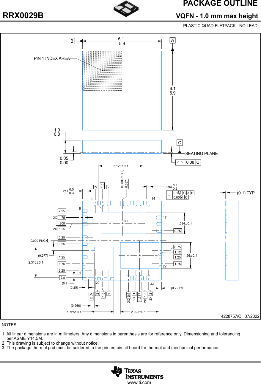
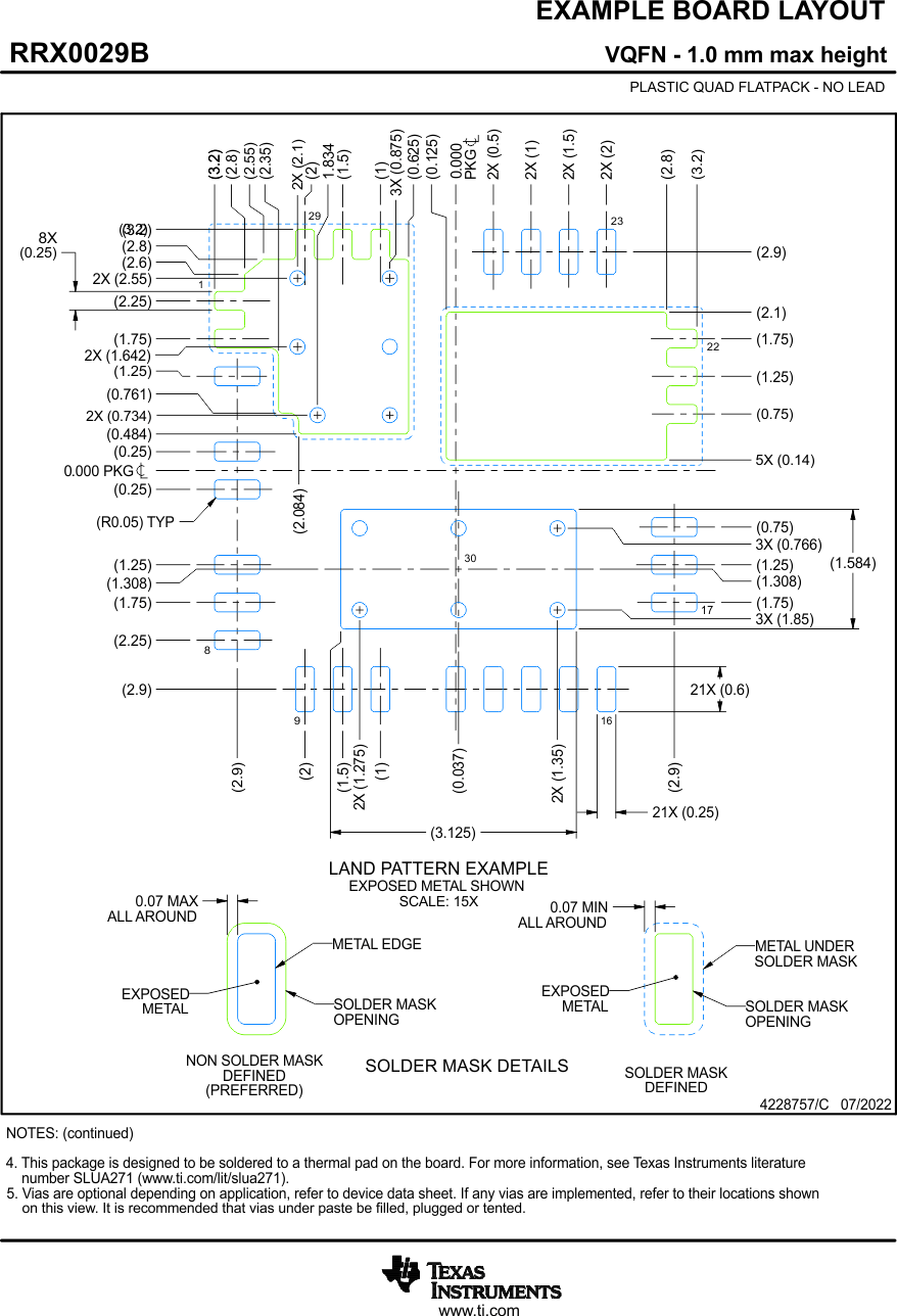
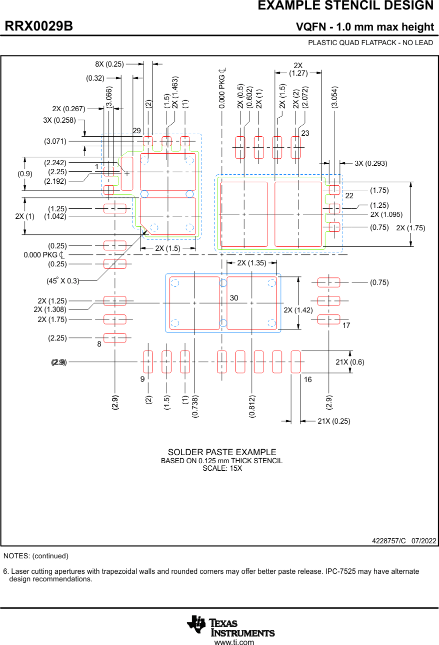
- 11Mechanical, Packaging, and Orderable Information
Package Options
Mechanical Data (Package|Pins)
- RRX|29
Thermal pad, mechanical data (Package|Pins)
Orderable Information
11.1 Tape and Reel Information
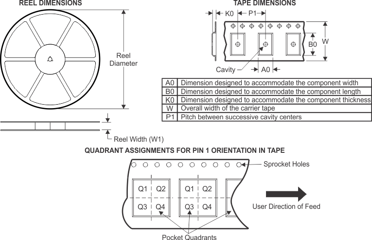
| Device | Package Type |
Package Drawing | Pins | SPQ | Reel Diameter (mm) |
Reel Width W1 (mm) |
A0 (mm) |
B0 (mm) |
K0 (mm) |
P1 (mm) |
W (mm) |
Pin1 Quadrant |
|---|---|---|---|---|---|---|---|---|---|---|---|---|
| LM70840QRRXRQ1 | VQFN | RRX | 29 | 3000 | 330.0 | 12.4 | 3.8 | 5.8 | 1.2 | 8.0 | 12.0 | Q1 |
| LM70860QRRXRQ1 | VQFN | RRX | 29 | 3000 | 330.0 | 12.4 | 3.8 | 5.8 | 1.2 | 8.0 | 12.0 | Q1 |
| LM70880QRRXRQ1 | VQFN | RRX | 29 | 3000 | 330.0 | 12.4 | 3.8 | 5.8 | 1.2 | 8.0 | 12.0 | Q1 |
| PLM70880RRXRQ1 | VQFN | RRX | 29 | 490 | 330.0 | 12.4 | 3.8 | 5.8 | 1.2 | 8.0 | 12.0 | Q1 |
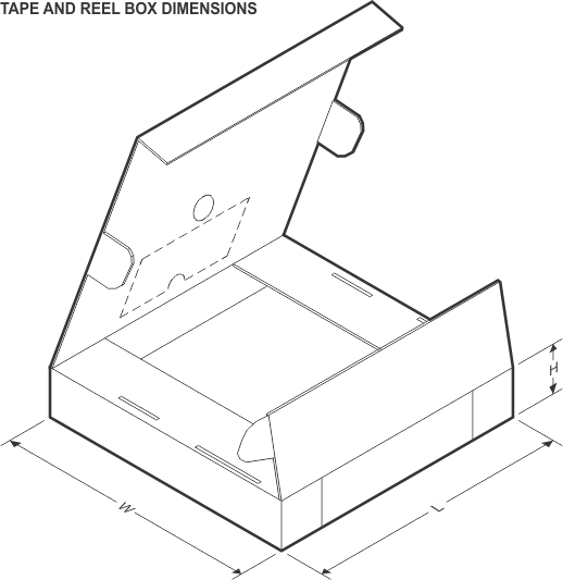
| Device | Package Type | Package Drawing | Pins | SPQ | Length (mm) | Width (mm) | Height (mm) |
|---|---|---|---|---|---|---|---|
| LM70840QRRXRQ1 | VQFN | RRX | 29 | 3000 | 367.0 | 367.0 | 35.0 |
| LM70860QRRXRQ1 | VQFN | RRX | 29 | 3000 | 367.0 | 367.0 | 35.0 |
| LM70880QRRXRQ1 | VQFN | RRX | 29 | 3000 | 367.0 | 367.0 | 35.0 |
| PLM70880RRXRQ1 | VQFN | RRX | 29 | 490 | 367.0 | 367.0 | 35.0 |