SNOSAV4B April 2008 – January 2016 LM7332
PRODUCTION DATA.
- 1 Features
- 2 Applications
- 3 Description
- 4 Revision History
- 5 Pin Configuration and Functions
- 6 Specifications
- 7 Detailed Description
- 8 Application and Implementation
- 9 Power Supply Recommendations
- 10Layout
- 11Device and Documentation Support
- 12Mechanical, Packaging, and Orderable Information
Package Options
Mechanical Data (Package|Pins)
Thermal pad, mechanical data (Package|Pins)
Orderable Information
8 Application and Implementation
NOTE
Information in the following applications sections is not part of the TI component specification, and TI does not warrant its accuracy or completeness. TI’s customers are responsible for determining suitability of components for their purposes. Customers should validate and test their design implementation to confirm system functionality.
8.1 Application Information
The LM7332 is a rail-to-rail input and output part with a slightly higher GBW of 20 MHz. It has current capability of 40-mA sourcing and 65-mA sinking, and can drive unlimited capacitive loads. The LM7332 is available in both VSSOP and SOIC packages.
8.1.1 Similar High Current Output Devices
The LM6172 has a higher GBW of 100 MHz and over 80 mA of current output. There is also a single version, the LM6171. The LM7372 has 120 MHz of GBW and 150 mA of current output. The LM7372 is available in an 8-pin SO PowerPAD™, and 16-pin SOIC packages with higher power dissipation.
The LME49600 buffer has 250 mA of current out and a 110-MHz bandwidth. The LME49600 is available in a DDPAK/TO-263 package for higher power dissipation.
Detailed information on these parts can be found at www.ti.com.
8.2 Typical Application
 Figure 50. Drive Amplifier for SAR ADC Schematic
8.2.1 Design Requirements
Assume a portable application requires the use of a 12-bit SAR ADC with acquisition time (tAQ) of 1 µs and sample and hold capacitance (CSH) of 80 pF.
The ADC runs on a single supply voltage of 5 V and has a full scale input of 2.5 VPP. A total harmonic distortion plus noise (THD+N) of less than –80 dB is required to maintain signal fidelity. Determine if the LM7332 is a suitable drive amplifier and find the values of Rflt and Cflt.
8.2.2 Detailed Design Procedure
The LM7332 can be used as a drive amplifier for SAR ADCs as shown in Figure 50.
The values of Rflt and Cflt depend on the ADC specifications as well as amplifier gain bandwidth product (GBWP) and output resistance (RO). It is also common to have a single ground-referenced supply voltage and sample signals up to half of the supply voltage with low distortion.
To determine whether or not the LM7332 is a suitable driver for this application, one must compare the settling time of the amplifier to the acquisition time of the ADC with Equation 1:
where
- GBWPmin: The minimum required gain bandwidth product of the drive amplifier
- N: Number of bits in ADC
- tAQ: The acquisition time of the ADC
Using a value of 12 bits for N and 1µs for tAQ, the GBWPmin must be greater than 5.7 MHz. The LM7332 has a GBWP of 21 MHz so it is indeed a suitable driver for this application.
Next, determine the value of Cflt with Equation 2:
where
- CSH: The ADC sample and hold capacitance
- Cflt: The external filter capacitance
Using a value of 80 pF for CSH, the value of Cflt must be between 1600 pF and 4800 pF. According to Figure 39, the LM7332 can drive a capacitive load of 2000 pF with 5 VPP and settle within 1 µs, therefore select 1800 pF as the nearest common capacitor value within the range.
Next determine the value of Rflt with Equation 3:
where
- Rflt: The external filter resistance
- Cflt: The external filter capacitance determined above
- GBWPmin: The minimum required gain bandwidth product of the drive amplifier determined above
- RO: The closed loop output impedance of the drive amplifier typically specified in the electrical characteristics table
Using a value of 1800 pF for Cflt, 5.7 MHz for GBWPmin, and a value of 3 Ω for RO the value of Rflt is determined to be 617.5 Ω. Use closest value of 620 Ω for a filter frequency (fflt) of 142 kHz given Equation 4:
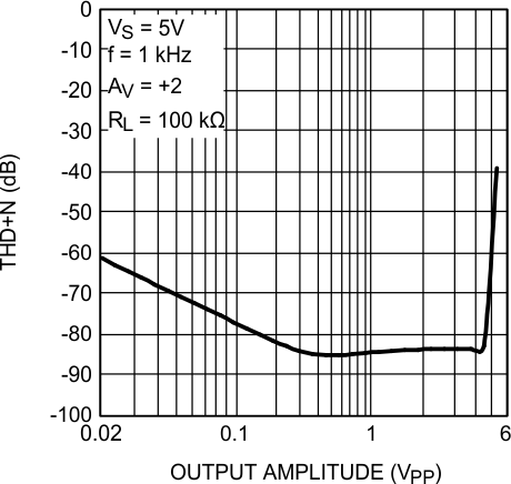
The last requirement is to drive input signals of 2.5 VPP on a single 5-V supply with THD+N less than –80 dB.
Figure 51 shows the THD+N response of the LM7332 with a single supply voltage of 5 V. The LM7332 can maintain THD+N levels as low as –83 dB for output levels up to 4 VPP. Therefore the final requirement has been met, and the LM7332 is a suitable drive amplifier for the 12-bit SAR ADC in this design example.
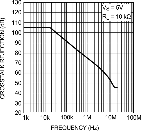
Driving two independent channels of the SAR ADC within minimal crosstalk between the channels may also be required. Figure 52 shows the crosstalk rejection over frequency. The LM7332 achieves 105 dB of crosstalk rejection up to 20 kHz and greater than 75 dB up to 1MHz which demonstrates the suitability of measuring very large input signals without interfering with adjacent channels.
8.2.3 Application Curves
 Figure 51. THD+N vs Output Amplitude
 Figure 52. Crosstalk Rejection vs. Frequency