SNOSAV4B April 2008 – January 2016 LM7332
PRODUCTION DATA.
- 1 Features
- 2 Applications
- 3 Description
- 4 Revision History
- 5 Pin Configuration and Functions
- 6 Specifications
- 7 Detailed Description
- 8 Application and Implementation
- 9 Power Supply Recommendations
- 10Layout
- 11Device and Documentation Support
- 12Mechanical, Packaging, and Orderable Information
Package Options
Mechanical Data (Package|Pins)
Thermal pad, mechanical data (Package|Pins)
Orderable Information
10 Layout
10.1 Layout Guidelines
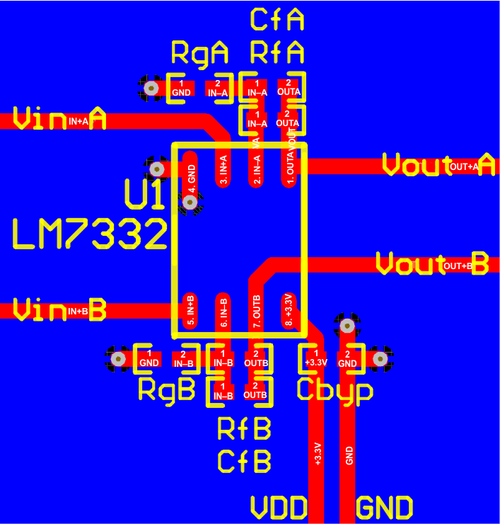
Take care to minimize the loop area formed by the bypass capacitor connection between supply pins and ground. A ground plane underneath the device is recommended; any bypass components to ground must have a nearby via to the ground plane. The optimum bypass capacitor placement is closest to the corresponding supply pin. Use of thicker traces from the bypass capacitors to the corresponding supply pins lowers the power supply inductance and provide a more stable power supply.
The feedback components must be placed as close to the device as possible to minimize stray parasitics.
10.2 Layout Example
 Figure 53. LM7332 Layout Example
10.3 Output Short Circuit Current and Dissipation Issues
The LM7332 output stage is designed for maximum output current capability. Even though momentary output shorts to ground and either supply can be tolerated at all operating voltages, longer-lasting short conditions can cause the junction temperature to rise beyond the absolute maximum rating of the device, especially at higher supply voltage conditions. Below a supply voltage of 6 V, the output short circuit condition can be tolerated indefinitely.
With the operational amplifier tied to a load, the device power dissipation consists of the quiescent power due to the supply current flow into the device, in addition to power dissipation due to the load current. The load portion of the power itself could include an average value (due to a DC load current) and an AC component. DC load current would flow if there is an output voltage offset, or the output AC average current is non-zero, or if the operational amplifier operates in a single-supply application where the output is maintained somewhere in the range of linear operation.
Therefore,
The operational amplifier quiescent power dissipation is calculated by Equation 6:
where
- IS: Supply Current
- VS: Total Supply Voltage (V+ − V−)
The DC load power is calculated by Equation 7:
where
- VO: Average Output Voltage
- Vr: V+ for sourcing and V− for sinking current
The AC load power is calculated as PAC = the value shown in Table 1.
Table 1 shows the maximum AC component of the load power dissipated by the operational amplifier for standard sinusoidal, triangular, and square waveforms:
Table 1. Normalized AC Power Dissipated in the Output Stage for Standard Waveforms
| PAC (W.Ω/V2) | ||
|---|---|---|
| SINUSOIDAL | TRIANGULAR | SQUARE |
| 50.7 x 10⁻³ | 46.9 x 10⁻³ | 62.5 x 10⁻³ |
The table entries are normalized to VS2/RL. To figure out the AC load current component of power dissipation, simply multiply the table entry corresponding to the output waveform by the factor VS2/RL. For example, with ±12-V supplies, a 600-Ω load, and triangular waveform power dissipation in the output stage is calculated as:
The maximum power dissipation allowed at a certain temperature is a function of maximum die junction temperature (TJ(MAX)) allowed, ambient temperature TA, and package thermal resistance from junction to ambient, RθJA.

For the LM7332, the maximum junction temperature allowed is 150°C at which no power dissipation is allowed. The power capability at 25°C is given by Equation 10 and Equation 11.
For VSSOP package:

For SOIC package:

Similarly, the power capability at 125°C is given by Equation 12 and Equation 13.
For VSSOP package:

For SOIC package:

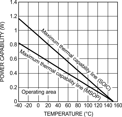
Figure 54 shows the power capability vs temperature for VSSOP and SOIC packages. The area under the maximum thermal capability line is the operating area for the device. When the device works in the operating area where PTOTAL is less than PD(MAX), the device junction temperature will remain below 150°C. If the intersection of ambient temperature and package power is above the maximum thermal capability line, the junction temperature will exceed 150°C, and this must be strictly prohibited.
 Figure 54. Power Capability vs Temperature
When high power is required and ambient temperature cannot be reduced, providing air flow is an effective approach to reduce thermal resistance therefore to improve power capability.