LM7372 High Speed, High Output Current, Dual Operational Amplifier
1 Features
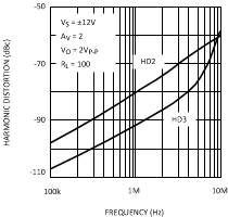
- −80 dBc Highest Harmonic Distortion @1 MHz, 2VPP
- Very High Slew Rate: 3000 V/µs
- Wide Gain Bandwidth Product: 120 MHz
- −3 dB Frequency @ AV = +2: 200 MHz
- Low Supply Current: 13 mA (both amplifiers)
- High Open Loop Gain: 85 dB
- High Output Current: 150 mA
- Differential Gain and Phase: 0.01%, 0.02°
2 Applications
- HDSL and ADSL Drivers
- Multimedia Broadcast Systems
- Professional Video Cameras
- CATV/Fiber Optics Signal Processing
- Pulse Amplifiers and Peak Detectors
- HDTV Amplifiers
3 Description
The LM7372 is a high speed dual voltage feedback amplifier with the slewing characteristic of current feedback amplifiers. However, it can be used in all traditional voltage feedback amplifier configurations.
The LM7372 is stable for gains as low as +2 or −1. It provides a very high slew rate at 3000 V/µs and a wide gain bandwidth product of 120 MHz, while consuming only 6.5 mA/per amplifier of supply current. It is ideal for video and high speed signal processing applications such as xDSL and pulse amplifiers. With 150 mA output current, the LM7372 can be used for video distribution, as a transformer driver or as a laser diode driver.
Operation on ±15 V power supplies allows for large signal swings and provides greater dynamic range and signal-to-noise ratio. The LM7372 offers high SFDR and low THD, ideal for ADC/DAC systems. In addition, the LM7372 is specified for ±5 V operation for portable applications.
The LM7372 is built on TI's Advance VIP™ III (Vertically integrated PNP) complementary bipolar process.
Device Information(1)
| PART NUMBER | PACKAGE | BODY SIZE (NOM) |
|---|---|---|
| LM7372 | DDA (8) | 4.90 mm × 3.91 mm |
| LM7372 | D (16) | 9.90 mm × 3.91 mm |
- For all available packages, see the orderable addendum at the end of the datasheet.
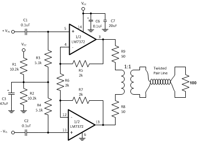
Single Supply Application (16-Pin SOIC)
Harmonic Distortion vs Frequency
4 Revision History
Changes from E Revision (March 2013) to F Revision
- Changed data sheet structure and organization. Added, updated, or renamed the following sections: Device Information Table, Pin Configuration and Functions, Application and Implementation; Device and Documentation Support; Mechanical, Packaging, and Ordering InformationGo
- Changed "Junction Temperature Range" to "Operating Temperature Range"Go
- Deleted TJ = 25°C for Electrical Characteristics tablesGo
Changes from D Revision (March 2013) to E Revision
- Changed layout of National Data Sheet to TI formatGo
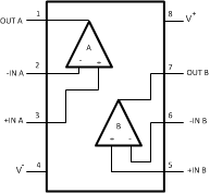
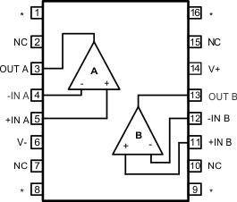
5 Pin Configuration and Functions
NOTE
For SO PowerPAD package the exposed pad should be tied either to V− or left electrically floating. Die attach material is conductive and is internally tied to V−.
Pin Functions
| PIN | I/O | DESCRIPTION | ||
|---|---|---|---|---|
| NAME | NUMBER | |||
| DDA | D | |||
| * | –– | 1,8,9,16 | –– | Heatsink Pin |
| -IN A | 2 | 4 | I | ChA Inverting Input |
| +IN A | 3 | 5 | I | ChA Non-inverting Input |
| -IN B | 6 | 12 | I | ChB Inverting Input |
| +IN B | 5 | 11 | I | ChB Non-inverting Input |
| NC | –– | 2, 7, 10, 15 | –– | No Connection |
| OUT A | 1 | 3 | O | Output A |
| OUT B | 7 | 13 | O | Output B |
| V- | 4 | 6 | I | Negative Supply |
| V+ | 8 | 14 | I | Positive Supply |
6 Specifications
6.1 Absolute Maximum Ratings(1)(3)(10)
over operating free-air temperature range (unless otherwise noted)| PARAMETER | MIN | MAX | UNIT | |
|---|---|---|---|---|
| Suppy Voltage (V+−V−) | 36 | V | ||
| Differential Input Voltage (VS = ±15V) | ±10 | V | ||
| Output Short Circuit to Ground(3) | Continuous | |||
| Soldering Information | Infrared or Convection Reflow (20 sec.) | 235 | °C | |
| Wave Soldering Lead Temperature (10 sec.) | 260 | °C | ||
| Input Voltage | V− to V+ | V | ||
| Maximum Junction Temperature(4) | 150 | °C | ||
6.2 Handling Ratings
| MIN | MAX | UNIT | |||
|---|---|---|---|---|---|
| Tstg | Storage temperature range | −65 | 150 | °C | |
| V(ESD) | Electrostatic discharge(2) | Human body model (HBM), per ANSI/ESDA/JEDEC JS-001, all pins(1) | 1500 | V | |
| Charged device model (CDM), per JEDEC specification JESD22-C101, all pins(2) | 200 | ||||
6.3 Recommended Operating Conditions(1)
over operating free-air temperature range (unless otherwise noted)| MIN | MAX | UNIT | ||
|---|---|---|---|---|
| Supply Voltage | 9 | 36 | V | |
| Operating Temperature Range | −40 | 85 | °C | |
6.4 Thermal Information
| THERMAL METRIC(1) | DDA | D | UNIT | |
|---|---|---|---|---|
| 8 PINS(4) | 16 PINS(4) | |||
| RθJA | Junction-to-ambient thermal resistance | 106 | 47 | °C/W |
6.5 ±15V DC Electrical Characteristics
Unless otherwise specified, all limits ensured for VCM = 0V and RL = 1kΩ. Boldface apply at the temperature extremes.| PARAMETER | TEST CONDITIONS | MIN(6) | TYP(5) | MAX(6) | UNIT | |
|---|---|---|---|---|---|---|
| VOS | Input Offset Voltage | 2.0 | 8.0 10.0 |
mV | ||
| TC VOS | Input Offset Voltage Average Drift | 12 | µV/°C | |||
| IB | Input Bias Current | 2.7 | 10 12 |
µA | ||
| IOS | Input Offset Current | 0.1 | 4.0 6.0 |
µA | ||
| RIN | Input Resistance | Common Mode | 40 | MΩ | ||
| Differential Mode | 3.3 | MΩ | ||||
| RO | Open Loop Output Resistance | 15 | Ω | |||
| CMRR | Common Mode Rejection Ratio | VCM = ±10V | 75 70 |
93 | dB | |
| PSRR | Power Supply Rejection Ratio | VS = ±15V to ±5V | 75 70 |
90 | dB | |
| VCM | Input Common-Mode Voltage Range | CMRR > 60dB | ±13 | V | ||
| AV | Large Signal Voltage Gain(7) | RL = 1kΩ | 75 70 |
85 | dB | |
| RL = 100Ω | 70 66 |
81 | dB | |||
| VO | Output Swing | RL = 1kΩ | 13 12.7 |
13.4 | V | |
| −13 −12.7 |
−13.3 | V | ||||
| IOUT = − 150mA | 11.8 11.4 |
12.4 | V | |||
| IOUT = 150mA | −11.2 −10.8 |
−11.9 | V | |||
| ISC | Output Short Circuit Current | Sourcing | 260 | mA | ||
| Sinking | 250 | mA | ||||
| IS | Supply Current (both Amps) | 13 | 17 19 |
mA |
6.6 ±15V AC Electrical Characteristics
Unless otherwise specified, all limits ensured for VCM = 0V and RL = 1kΩ. Boldface apply at the temperature extremes.| PARAMETER | TEST CONDITIONS | MIN(6) | TYP(5) | MAX(6) | UNIT | |
|---|---|---|---|---|---|---|
| SR | Slew Rate(8) | AV = +2, VIN 13VP-P | 3000 | V/µs | ||
| AV = +2, VIN 10VP-P | 2000 | |||||
| Unity Bandwidth Product | 120 | MHz | ||||
| −3dB Frequency | AV = +2 | 220 | MHz | |||
| φm | Phase Margin | AVOL = 6dB | 70 | deg | ||
| tS | Settling Time (0.1%) | AV = −1, AO = ±5V, RL = 500Ω |
50 | ns | ||
| tP | Propagation Delay | AV = −2, VIN = ±5V, RL = 500Ω |
6.0 | ns | ||
| AD | Differential Gain(9) | 0.01% | ||||
| φD | Differential Phase(9) | 0.02 | deg | |||
| hd2 | Second Harmonic Distortion FIN = 1MHz, AV = +2 |
VOUT = 2VP-P, RL = 100Ω | −80 | dBc | ||
| VOUT = 16.8VP-P, RL = 100Ω | −73 | dBc | ||||
| hd3 | Third Harmonic Distortion FIN = 1MHz, AV = +2 |
VOUT = 2VP-P, RL = 100Ω | −91 | dBc | ||
| VOUT = 16.8VP-P, RL = 100Ω | −67 | dBc | ||||
| IMD | Intermodulation Distortion | Fin 1 = 75kHz, Fin 2 = 85kHz VOUT = 16.8VP-P, RL = 100Ω |
−87 | dBc | ||
| en | Input-Referred Voltage Noise | f = 10kHz | 14 | nV/√Hz | ||
| in | Input-Referred Current Noise | f = 10kHz | 1.5 | pA/√Hz |
6.7 ±5V DC Electrical Characteristics
Unless otherwise specified, all limits ensured for VCM = 0V and RL = 1kΩ. Boldface apply at the temperature extremes.| PARAMETER | TEST CONDITIONS | MIN(6) | TYP(5) | MAX(6) | UNIT | |
|---|---|---|---|---|---|---|
| VOS | Input Offset Voltage | 2.2 | 8.0 10.0 |
mV | ||
| TC VOS | Input Offset Voltage Average Drift | 12 | µV/°C | |||
| IB | Input Bias Current | 3.3 | 10 12 |
µA | ||
| IOS | Input Offset Current | 0.1 | 4 6 |
µA | ||
| RIN | Input Resistance | Common Mode | 40 | MΩ | ||
| Differential Mode | 3.3 | MΩ | ||||
| RO | Open Loop Output Resistance | 15 | Ω | |||
| CMRR | Common Mode Rejection Ratio | VCM = ±2.5V | 70 65 |
90 | dB | |
| PSRR | Power Supply Rejection Ratio | VS = ±15V to ±5V | 75 70 |
90 | dB | |
| VCM | Input Common-Mode Voltage Range | CMRR > 60dB | ±3 | V | ||
| AV | Large Signal Voltage Gain(7) | RL = 1kΩ | 70 65 |
78 | dB | |
| RL = 100Ω | 64 60 |
72 | dB | |||
| VO | Output Swing | RL = 1kΩ | 3.2 3.0 |
3.4 | V | |
| −3.2 −3.0 |
−3.4 | V | ||||
| IOUT = − 80mA | 2.5 2.2 |
2.8 | V | |||
| IOUT = 80mA | −2.5 −2.2 |
−2.7 | V | |||
| ISC | Output Short Circuit Current | Sourcing | 150 | mA | ||
| Sinking | 150 | mA | ||||
| IS | Supply Current (both Amps) | 12.4 | 16 18 |
mA |
6.8 ±5V AC Electrical Characteristics
Unless otherwise specified, all limits ensured for VCM = 0V and RL = 1kΩ. Boldface apply at the temperature extremes.| PARAMETER | TEST CONDITIONS | MIN(6) | TYP(5) | MAX(6) | UNIT | |
|---|---|---|---|---|---|---|
| SR | Slew Rate(8) | AV = +2, VIN 3VP-P | 700 | V/µs | ||
| Unity Bandwidth Product | 100 | MHz | ||||
| −3dB Frequency | AV = +2 | 125 | MHz | |||
| φm | Phase Margin | 70 | deg | |||
| tS | Settling Time (0.1%) | AV = −1, VO = ±1V, RL = 500Ω | 70 | ns | ||
| tP | Propagation Delay | AV = +2, VIN = ±1V, RL = 500Ω | 7 | ns | ||
| AD | Differential Gain(9) | 0.02% | ||||
| φD | Differential Phase(9) | 0.03 | deg | |||
| hd2 | Second Harmonic Distortion FIN = 1MHz, AV = +2 |
VOUT = 2VP-P, RL = 100Ω | −84 | dBc | ||
| hd3 | Third Harmonic Distortion FIN = 1MHz, AV = +2 |
VOUT = 2VP-P, RL = 100Ω | −94 | dBc | ||
| en | Input-Referred Voltage Noise | f = 10kHz | 14 | nV/√Hz | ||
| in | Input-Referred Current Noise | f = 10kHz | 1.8 | pA/√Hz |
