SNOSD62 June 2017 LM741-MIL
PRODUCTION DATA.
- 1 Features
- 2 Applications
- 3 Description
- 4 Revision History
- 5 Pin Configuration and Functions
- 6 Specifications
- 7 Detailed Description
- 8 Application and Implementation
- 9 Power Supply Recommendations
- 10Layout
- 11Device and Documentation Support
- 12Mechanical, Packaging, and Orderable Information
Package Options
Mechanical Data (Package|Pins)
Thermal pad, mechanical data (Package|Pins)
Orderable Information
5 Pin Configuration and Functions
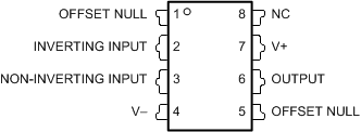
P Package
8-Pin PDIP
Top View

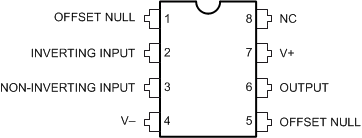
NAB Package
8-Pin CDIP
Top View

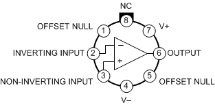
LMC Package
8-Pin TO-99
Top View

Pin Functions
| PIN | I/O | DESCRIPTION | |
|---|---|---|---|
| NAME | NO. | ||
| INVERTING INPUT | 2 | I | Inverting signal input |
| NC | 8 | N/A | No Connect, leave floating |
| NONINVERTING INPUT | 3 | I | Noninverting signal input |
| OFFSET NULL | 1 | I | Offset null pin used to eliminate the offset voltage and balance the input voltages. |
| OFFSET NULL | 5 | ||
| OUTPUT | 6 | O | Amplified signal output |
| V+ | 7 | I | Positive supply voltage |
| V– | 4 | I | Negative supply voltage |