SLVSFD0
September 2019
LM74202-Q1
PRODUCTION DATA.
1
Features
2
Applications
3
Description
Device Images
Simplified Schematic
ISO16750-2 Load Dump Pulse 5b Performance at 12 V
4
Revision History
5
Pin Configuration and Functions
Pin Functions
6
Specifications
6.1
Absolute Maximum Ratings
6.2
ESD Ratings
6.3
Recommended Operating Conditions
Table 1.
Thermal Information
6.4
Electrical Characteristics
6.5
Timing Requirements
6.6
Typical Characteristics
7
Parameter Measurement Information
8
Detailed Description
8.1
Overview
8.2
Functional Block Diagram
8.3
Feature Description
8.3.1
Undervoltage Lockout (UVLO)
8.3.2
Overvoltage Protection (OVP)
8.3.3
Reverse Battery Protection
8.3.4
Hot Plug-In and In-Rush Current Control
8.3.5
Overload and Short Circuit Protection
8.3.5.1
Overload Protection
8.3.5.1.1
Active Current Limiting
8.3.5.1.2
Electronic Circuit Breaker with Overload Timeout, MODE = OPEN
8.3.5.2
Short Circuit Protection
8.3.5.2.1
Start-Up With Short-Circuit On Output
8.3.5.3
FAULT Response
8.3.5.3.1
Look Ahead Overload Current Fault Indicator
8.3.5.4
Current Monitoring
8.3.5.5
IN, OUT, RTN and GND Pins
8.3.5.6
Thermal Shutdown
8.3.5.7
Low Current Shutdown Control (SHDN)
8.4
Device Functional Modes
9
Application and Implementation
9.1
Application Information
9.2
Typical Application
9.2.1
Design Requirements
9.2.2
Detailed Design Procedure
9.2.2.1
Step by Step Design Procedure
9.2.2.2
Setting Undervoltage Lockout and Overvoltage Set Point for Operating Voltage Range
9.2.2.3
Programming the Current-Limit Threshold—R(ILIM) Selection
9.2.2.4
Programming Current Monitoring Resistor—RIMON
9.2.2.5
Limiting the Inrush Current
9.2.2.5.1
Selection of Input TVS for Transient Protection
9.2.3
Application Curves
10
Power Supply Recommendations
10.1
Transient Protection
11
Layout
11.1
Layout Guidelines
11.2
Layout Example
12
Device and Documentation Support
12.1
Documentation Support
12.1.1
Related Documentation
12.2
Receiving Notification of Documentation Updates
12.3
Community Resources
12.4
Trademarks
12.5
Electrostatic Discharge Caution
12.6
Glossary
13
Mechanical, Packaging, and Orderable Information
Package Options
Mechanical Data (Package|Pins)
PWP|16
MPDS371A
Thermal pad, mechanical data (Package|Pins)
PWP|16
PPTD333C
Orderable Information
slvsfd0_oa
slvsfd0_pm
11.2
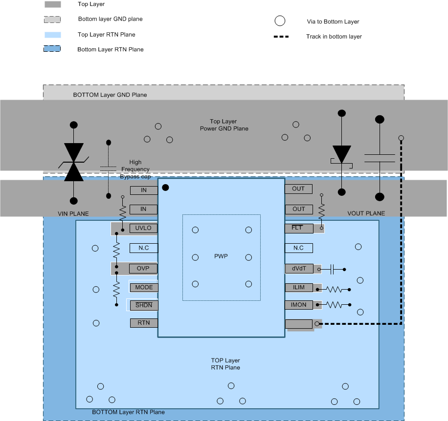
Layout Example
Figure 47.
Typical PCB Layout Example With HTSSOP Package With a 2-Layer PCB