SLVSFD0 September   2019 LM74202-Q1

PRODUCTION DATA.  

  1. Features
  2. Applications
  3. Description
    1.     Device Images
      1.      Simplified Schematic
      2.      ISO16750-2 Load Dump Pulse 5b Performance at 12 V
  4. Revision History
  5. Pin Configuration and Functions
    1.     Pin Functions
  6. Specifications
    1. 6.1      Absolute Maximum Ratings
    2. 6.2      ESD Ratings
    3. 6.3      Recommended Operating Conditions
    4. Table 1. Thermal Information
    5. 6.4      Electrical Characteristics
    6. 6.5      Timing Requirements
    7. 6.6      Typical Characteristics
  7. Parameter Measurement Information
  8. Detailed Description
    1. 8.1 Overview
    2. 8.2 Functional Block Diagram
    3. 8.3 Feature Description
      1. 8.3.1 Undervoltage Lockout (UVLO)
      2. 8.3.2 Overvoltage Protection (OVP)
      3. 8.3.3 Reverse Battery Protection
      4. 8.3.4 Hot Plug-In and In-Rush Current Control
      5. 8.3.5 Overload and Short Circuit Protection
        1. 8.3.5.1 Overload Protection
          1. 8.3.5.1.1 Active Current Limiting
          2. 8.3.5.1.2 Electronic Circuit Breaker with Overload Timeout, MODE = OPEN
        2. 8.3.5.2 Short Circuit Protection
          1. 8.3.5.2.1 Start-Up With Short-Circuit On Output
        3. 8.3.5.3 FAULT Response
          1. 8.3.5.3.1 Look Ahead Overload Current Fault Indicator
        4. 8.3.5.4 Current Monitoring
        5. 8.3.5.5 IN, OUT, RTN and GND Pins
        6. 8.3.5.6 Thermal Shutdown
        7. 8.3.5.7 Low Current Shutdown Control (SHDN)
    4. 8.4 Device Functional Modes
  9. Application and Implementation
    1. 9.1 Application Information
    2. 9.2 Typical Application
      1. 9.2.1 Design Requirements
      2. 9.2.2 Detailed Design Procedure
        1. 9.2.2.1 Step by Step Design Procedure
        2. 9.2.2.2 Setting Undervoltage Lockout and Overvoltage Set Point for Operating Voltage Range
        3. 9.2.2.3 Programming the Current-Limit Threshold—R(ILIM) Selection
        4. 9.2.2.4 Programming Current Monitoring Resistor—RIMON
        5. 9.2.2.5 Limiting the Inrush Current
          1. 9.2.2.5.1 Selection of Input TVS for Transient Protection
      3. 9.2.3 Application Curves
  10. 10Power Supply Recommendations
    1. 10.1 Transient Protection
  11. 11Layout
    1. 11.1 Layout Guidelines
    2. 11.2 Layout Example
  12. 12Device and Documentation Support
    1. 12.1 Documentation Support
      1. 12.1.1 Related Documentation
    2. 12.2 Receiving Notification of Documentation Updates
    3. 12.3 Community Resources
    4. 12.4 Trademarks
    5. 12.5 Electrostatic Discharge Caution
    6. 12.6 Glossary
  13. 13Mechanical, Packaging, and Orderable Information

Package Options

Mechanical Data (Package|Pins)
Thermal pad, mechanical data (Package|Pins)
Orderable Information

Typical Characteristics

TA = 25 °C, V(IN) = 12 V, V(SHDN)= 2 V, R(ILIM) = 120 kΩ, IMON = FLT = OPEN, C(IN) = 0.1 μF, C(OUT) = 1 μF, C(dVdT) = OPEN. (Unless otherwise noted)
LM74202-Q1 D001_SLVSEM1.gif
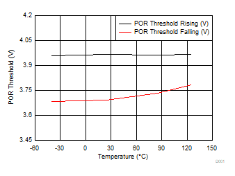
Figure 1. POR Threshold (VPOR) vs Temperature
LM74202-Q1 D003_SLVSFD0.gif
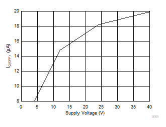
Figure 3. Supply Current OFF (IQOFF) vs Supply Voltage (VIN)
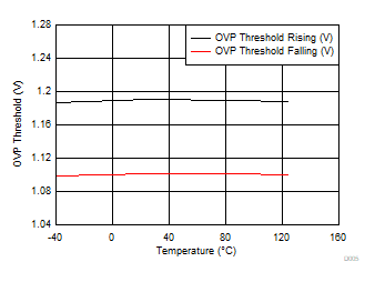
LM74202-Q1 D005_SLVSEM1.gif
Figure 5. OVP Thresholds (VOVPR, VOVPF) vs Temperature
LM74202-Q1 D007_SLVSEM1.gif
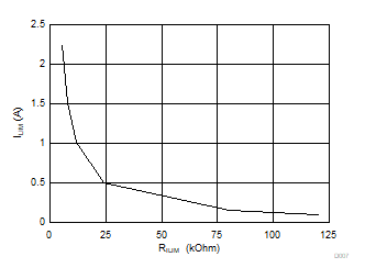
Figure 7. ILIM vs RILIM
LM74202-Q1 D009_SLVSEM1.gif
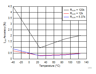
Figure 9. ILIM Accuracy vs Temperature with VIN = 12 V
LM74202-Q1 D011_SLVSEM1.gif
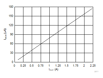
Figure 11. IMON vs IOUT
LM74202-Q1 D013_SLVSEM1.gif
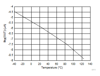
V(OUT) = 24 V V(IN) = 0 V VSHDN = 0 V
Figure 13. Ilkg(OUT) vs Temperature with VIN = 0 V
LM74202-Q1 D015_SLVSEM1.gif
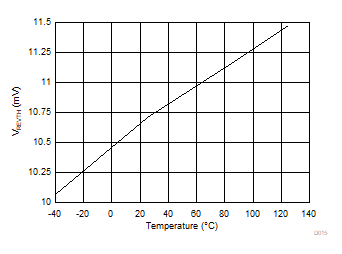
Figure 15. VREVTH vs Temperature
LM74202-Q1 D017_SLVSEM1.gif
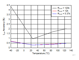
Figure 17. ILIM Accuracy vs Temperature with VIN = 24 V
LM74202-Q1 D002_SLVSFD0.gif
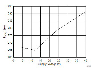
Figure 2. Supply Current ON (IQON) vs Supply Voltage (VIN)
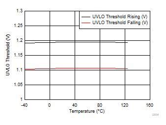
LM74202-Q1 D004_SLVSEM1.gif
Figure 4. UVLO Thresholds (VUVLOR, VUVLOF) vs Temperature
LM74202-Q1 D006_SLVSEM1.gif
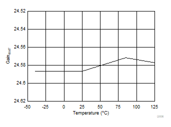
Figure 6. GAIN(dVdT) vs Temperature
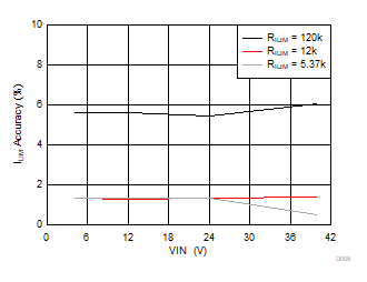
LM74202-Q1 D008_SLVSFD0.gif
TA = -40 to 125 °C
Figure 8. ILIM Accuracy vs Supply Voltage
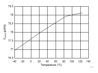
LM74202-Q1 D010_SLVSEM1.gif
Figure 10. GAIN(IMON) vs Temperature
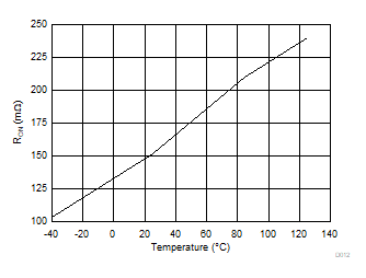
LM74202-Q1 D012_SLVSEM1.gif
Figure 12. RON vs Temperature
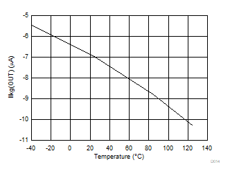
LM74202-Q1 D014_SLVSEM1.gif
V(OUT) = 0 V V(IN) = –24 V VSHDN = 0 V
Figure 14. Ilkg(OUT) vs Temperature with VIN = –24 V
LM74202-Q1 D016_SLVSEM1.gif
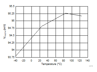
Figure 16. VFWDTH vs Temperature
LM74202-Q1 D018_SLVSEM1.gif
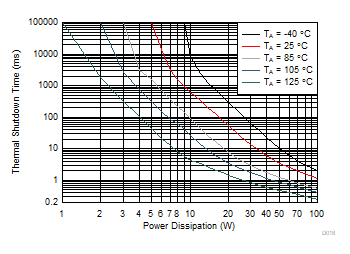
Taken on 2-layer PCB with 0.07-mm thick copper and copper area of 10.5 cm2 connected to PowerPAD.
Figure 18. Thermal Shutdown Time vs Power Dissipation