SNOSDD6 September 2021 LM74700-EP
PRODUCTION DATA
- 1 Features
- 2 Applications
- 3 Description
- 4 Revision History
- 5 Pin Configuration and Functions
- 6 Specifications
- 7 Parameter Measurement Information
- 8 Detailed Description
-
9 Application and Implementation
- 9.1 Application Information
- 9.2 Typical Application
- 9.3 OR-ing Application Configuration
- 10Power Supply Recommendations
- 11Layout
- 12Device and Documentation Support
- 13Mechanical, Packaging, and Orderable Information
Package Options
Mechanical Data (Package|Pins)
- DDF|8
Thermal pad, mechanical data (Package|Pins)
Orderable Information
9.3 OR-ing Application Configuration
Basic redundant power architecture comprises of two or more voltage or power supply sources driving a single load. In its simplest form, the OR-ing solution for redundant power supplies consists of Schottky OR-ing diodes that protect the system against an input power supply fault condition. A diode OR-ing device provides effective and low cost solution with few components. However, the diodes forward voltage drops affects the efficiency of the system permanently, since each diode in an OR-ing application spends most of its time in forward conduction mode. These power losses increase the requirements for thermal management and allocated board space.
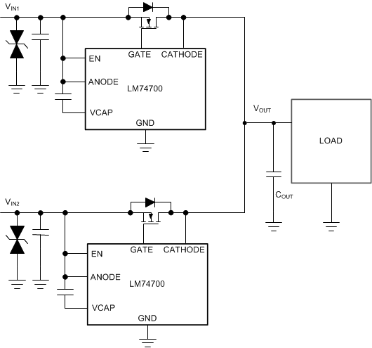
The LM74700-EP ICs combined with external N-Channel MOSFETs can be used in OR-ing Solution as shown in Figure 9-18. The forward diode drop is reduced as the external N-Channel MOSFET is turned ON during normal operation. LM74700-EP quickly detects the reverse current, pulls down the MOSFET gate fast, leaving the body diode of the MOSFET to block the reverse current flow. An effective OR-ing solution needs to be extremely fast to limit the reverse current amount and duration. The LM74700-EP devices in OR-ing configuration constantly sense the voltage difference between Anode and Cathode pins, which are the voltage levels at the power sources (VIN1, VIN2) and the common load point respectively. The source to drain voltage VDS for each MOSFET is monitored by the Anode and Cathode pins of the LM74700-EP. A fast comparator shuts down the Gate Drive through a fast pull-down within 0.45 μs (typical) as soon as V(IN) – V(OUT) falls below –11 mV. The fast comparator turns on the Gate with 11-mA gate charge current once the differential forward voltage V(IN) – V(OUT) exceeds 50 mV.
 Figure 9-18 Typical OR-ing Application
Figure 9-12 to Figure 9-15 show the smooth switch over between two power supply rails VIN1 at 28 V and VIN2 at 33 V. Figure 9-16 and Figure 9-17 illustrate the performance when VIN2 fails. LM74700-EP controlling VIN2 power rail turns off quickly, so that the output remains uninterrupted and VIN1 is protected from VIN2 failure.