SNOSDD6 September 2021 LM74700-EP
PRODUCTION DATA
- 1 Features
- 2 Applications
- 3 Description
- 4 Revision History
- 5 Pin Configuration and Functions
- 6 Specifications
- 7 Parameter Measurement Information
- 8 Detailed Description
-
9 Application and Implementation
- 9.1 Application Information
- 9.2 Typical Application
- 9.3 OR-ing Application Configuration
- 10Power Supply Recommendations
- 11Layout
- 12Device and Documentation Support
- 13Mechanical, Packaging, and Orderable Information
Package Options
Mechanical Data (Package|Pins)
- DDF|8
Thermal pad, mechanical data (Package|Pins)
Orderable Information
3 Description
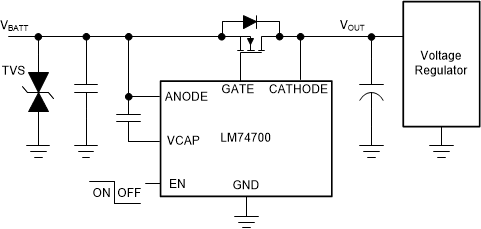
The LM74700-EP is an ideal diode controller which operates in conjunction with an external N-channel MOSFET as an ideal diode rectifier for low loss reverse polarity protection with a 20-mV forward voltage drop. The wide supply input range of 3.2 V to 65 V allows control of many popular DC bus voltages such as 12-V, 24-V and 48-V systems. The device can withstand and protect the loads from negative supply voltages down to –65 V.
The device controls the GATE of the MOSFET to regulate the forward voltage drop at 20 mV. The regulation scheme enables graceful turn off of the MOSFET during a reverse current event and ensures zero DC reverse current flow. Fast response (< 0.75 µs) to Reverse Current Blocking makes the device suitable for systems with output voltage holdup requirements during power fail and input micro-short conditions.
The LM74700-EP controller provides a charge pump gate drive for an external N-channel MOSFET. The high voltage rating of LM74700-EP helps to simplify the system designs for automotive ISO7637 protection. With the enable pin low, the controller is off and draws approximately 1 µA of current. The LM74700-EP is fully specified over the temperature range of TA = –55°C to +125°C.
| PART NUMBER | PACKAGE | BODY SIZE (NOM) |
|---|---|---|
| LM74700-EP | SOT-23 (8) | 2.90 mm × 1.60 mm |
 Typical Application Schematic
 Reverse Current Blocking During Input Short