SNOSDF5 September   2023 LM74700D-Q1

PRODUCTION DATA  

  1.   1
  2. Features
  3. Applications
  4. Description
  5. Revision History
  6. Pin Configuration and Functions
  7. Specifications
    1. 6.1 Absolute Maximum Ratings
    2. 6.2 ESD Ratings
    3. 6.3 Recommended Operating Conditions
    4. 6.4 Thermal Information
    5. 6.5 Electrical Characteristics
    6. 6.6 Switching Characteristics
  8. Typical Characteristics
  9. Parameter Measurement Information
  10. Detailed Description
    1. 9.1 Overview
    2. 9.2 Functional Block Diagram
    3. 9.3 Feature Description
      1. 9.3.1 Input Voltage
      2. 9.3.2 Charge Pump
      3. 9.3.3 Gate Driver
      4. 9.3.4 Enable
    4. 9.4 Device Functional Modes
      1. 9.4.1 Shutdown Mode
      2. 9.4.2 Conduction Mode
        1. 9.4.2.1 Regulated Conduction Mode
        2. 9.4.2.2 Full Conduction Mode
        3. 9.4.2.3 Reverse Current Protection Mode
  11. 10Application and Implementation
    1. 10.1 Application Information
    2. 10.2 Typical Application
      1. 10.2.1 Design Requirements
      2. 10.2.2 Detailed Design Procedure
        1. 10.2.2.1 Design Considerations
        2. 10.2.2.2 MOSFET Selection
        3. 10.2.2.3 Charge Pump VCAP, Input and Output Capacitance
      3. 10.2.3 Selection of TVS Diodes for 12-V Battery Protection Applications
      4. 10.2.4 Selection of TVS Diodes and MOSFET for 24-V Battery Protection Applications
      5. 10.2.5 Application Curves
      6. 10.2.6 OR-ing Application Configuration
    3. 10.3 Power Supply Recommendations
    4. 10.4 Layout
      1. 10.4.1 Layout Guidelines
      2. 10.4.2 Layout Example
  12. 11Device and Documentation Support
    1. 11.1 Receiving Notification of Documentation Updates
    2. 11.2 Support Resources
    3. 11.3 Trademarks
    4. 11.4 Electrostatic Discharge Caution
    5. 11.5 Glossary
  13. 12Mechanical, Packaging, and Orderable Information

Package Options

Mechanical Data (Package|Pins)
Thermal pad, mechanical data (Package|Pins)
Orderable Information

Application Curves

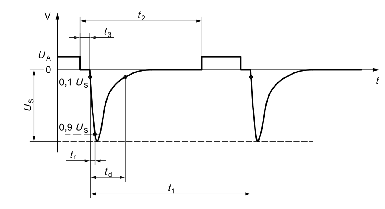
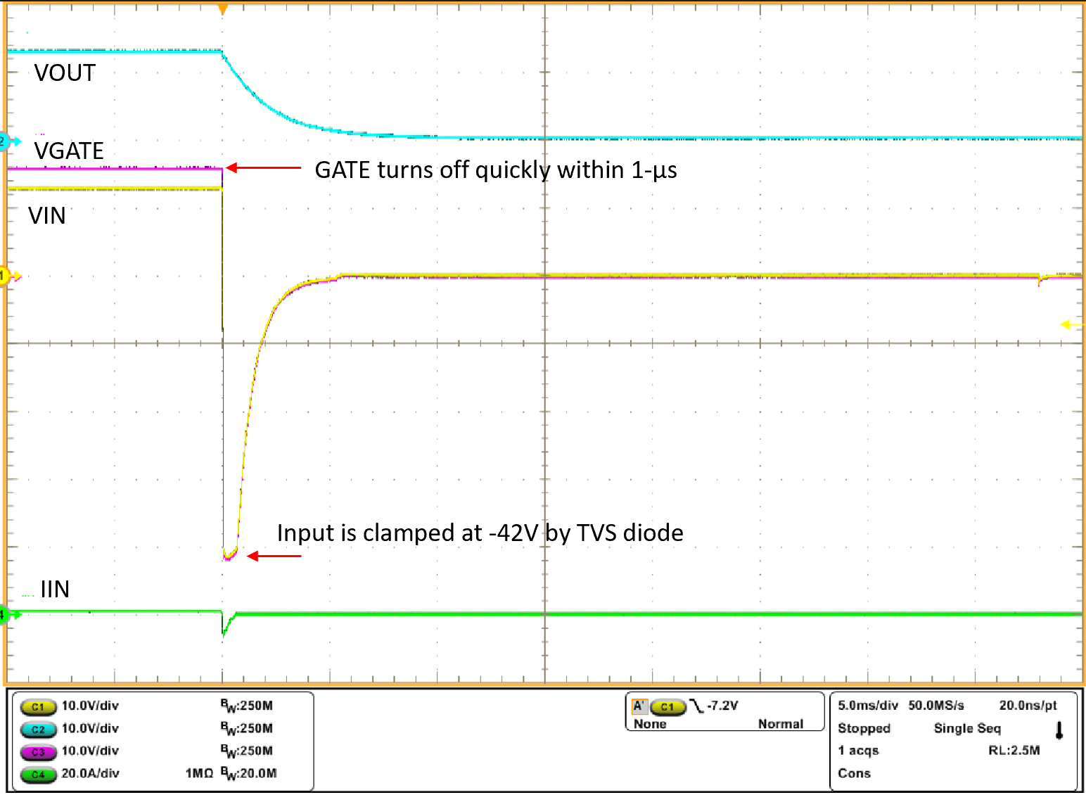
GUID-00111DEC-7E81-46C0-A81B-065F034B7CB0-low.pngFigure 10-4 ISO 7637-2 Pulse 1
GUID-20230814-SS0I-HJP9-VPQH-RW7TD4DBJNT9-low.png
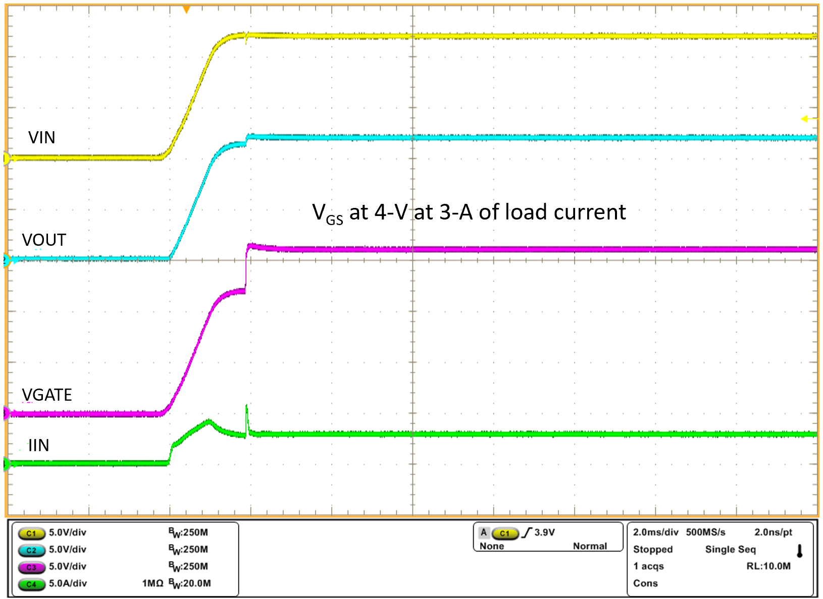
Time (2 ms/DIV)
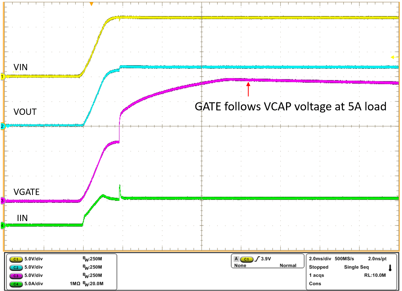
Figure 10-6 Start-Up With 3-A Load
GUID-20230814-SS0I-NHGX-ZSPV-4WTKCWNQCCGR-low.png
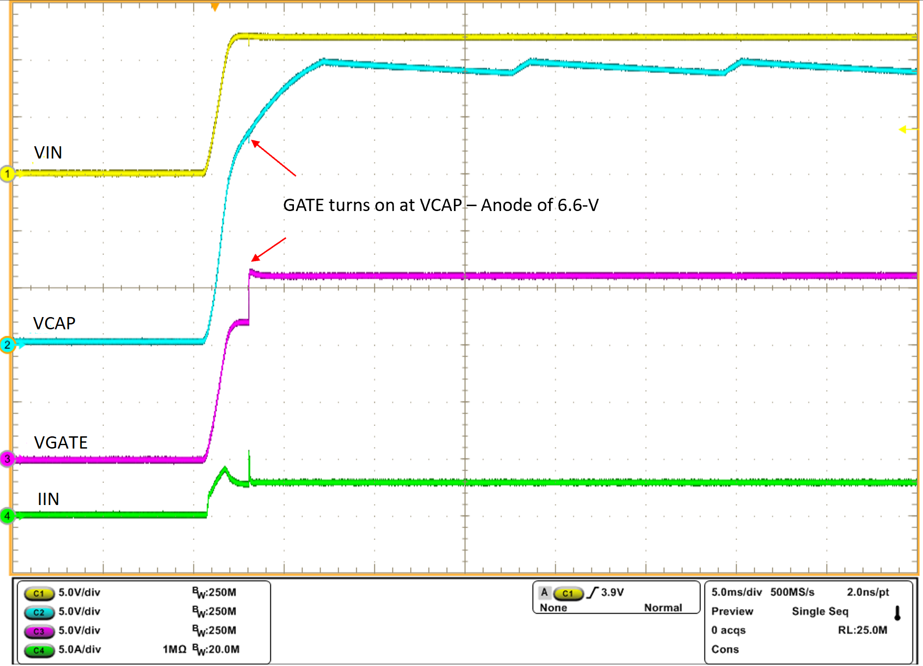
Time (5 ms/DIV)
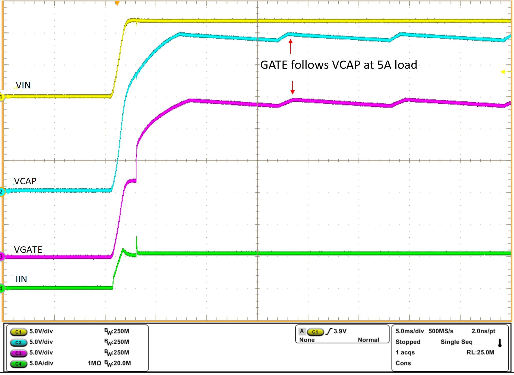
Figure 10-8 VCAP During Start-Up at 3-A Load
GUID-20230814-SS0I-B9JK-9XWZ-9C2QK5KB754J-low.png
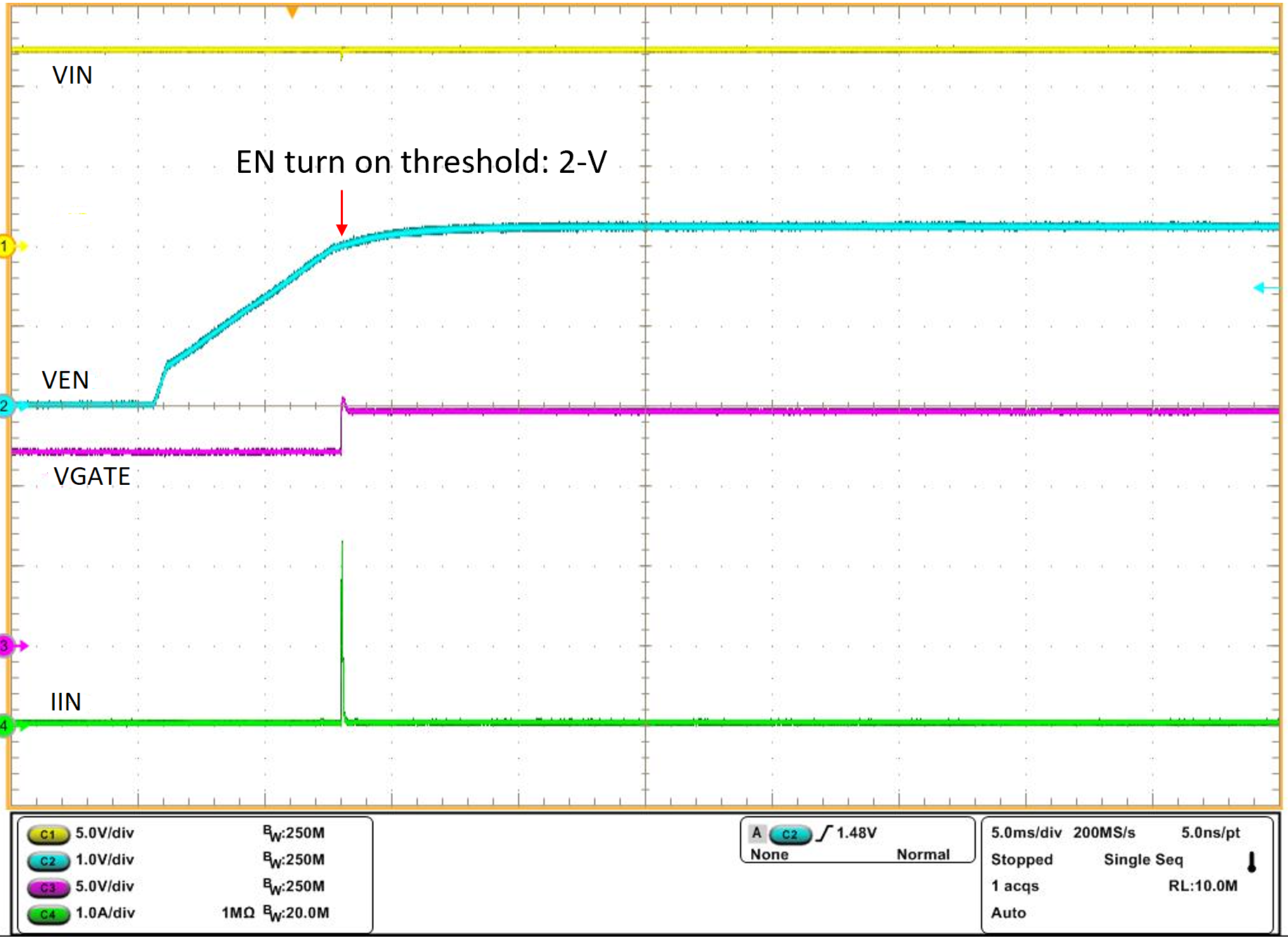
Time (5 ms/DIV)
Figure 10-10 Enable Threshold
GUID-20230814-SS0I-JC71-CCP1-X3Z7HBZ2LHWQ-low.png
Time (5 ms/DIV)
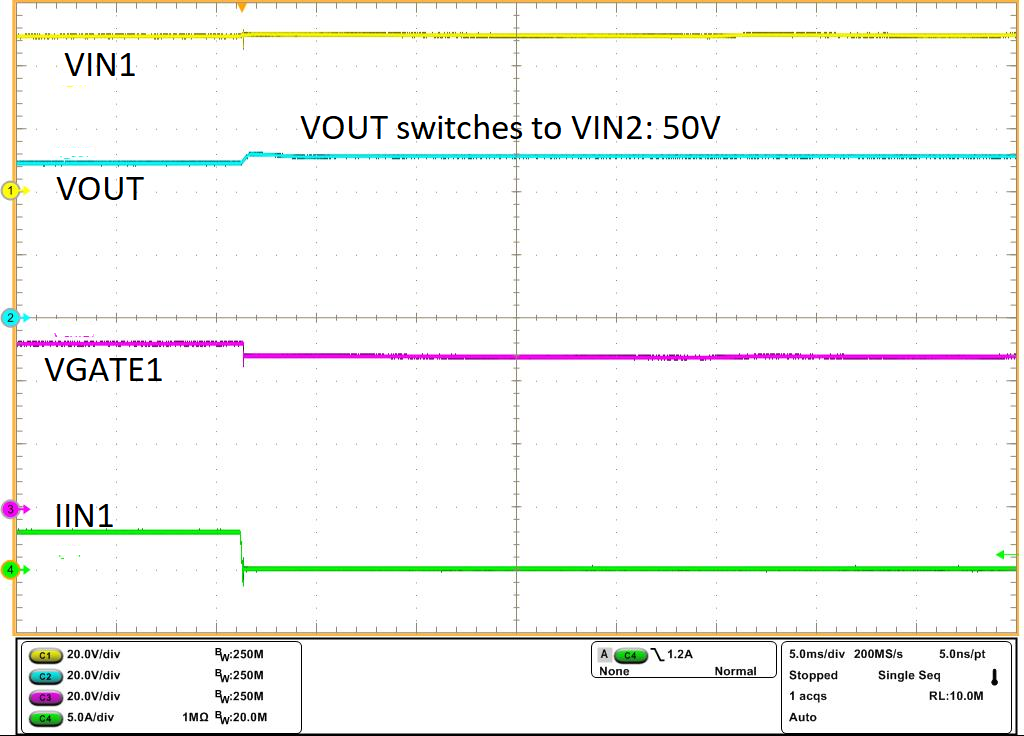
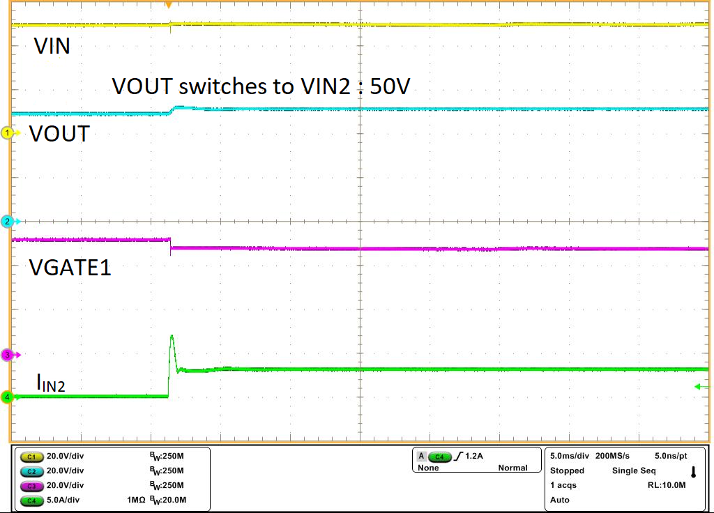
Figure 10-12 OR-ing VIN1 to VIN2 Switch Over
GUID-20230912-SS0I-6WTK-CBTK-QM4NPMMLHSWF-low.png
Time (5 ms/DIV)
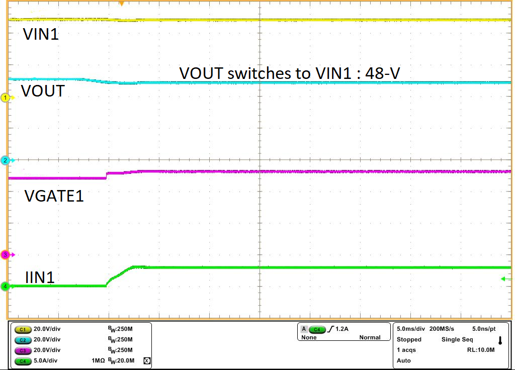
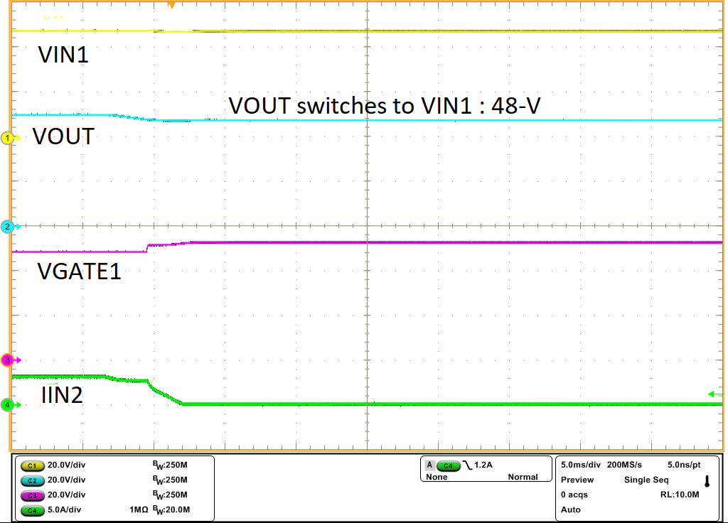
Figure 10-14 OR-ing VIN2 to VIN1 Switch Over
GUID-20230912-SS0I-CHLT-FPDN-FRXWJSWZRSXQ-low.jpg
Time (5 ms/DIV)
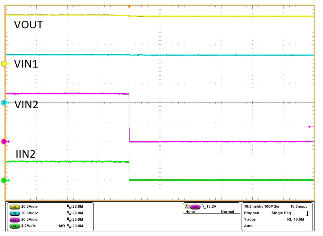
Figure 10-16 OR-ing - VIN2 Failure and Switch Over to VIN1
GUID-20230816-SS0I-H0XK-Z8F7-K7P2BWP1FRZZ-low.png
Time (5 ms/DIV)
Figure 10-5 Response to ISO 7637-2 Pulse 1
GUID-20230814-SS0I-1RZP-3WHK-R9JX8HR5VDS3-low.png
Time (2 ms/DIV)
Figure 10-7 Start-Up With 5-A Load
GUID-20230814-SS0I-0XNP-W5BB-WVS6DLJV0LRN-low.png
Time (5 ms/DIV)
Figure 10-9 VCAP During Start-Up at 5.8-A Load
GUID-20230912-SS0I-BZVB-VQGC-SHLS5QV0NTQ9-low.jpg
Time (100 µs/DIV)
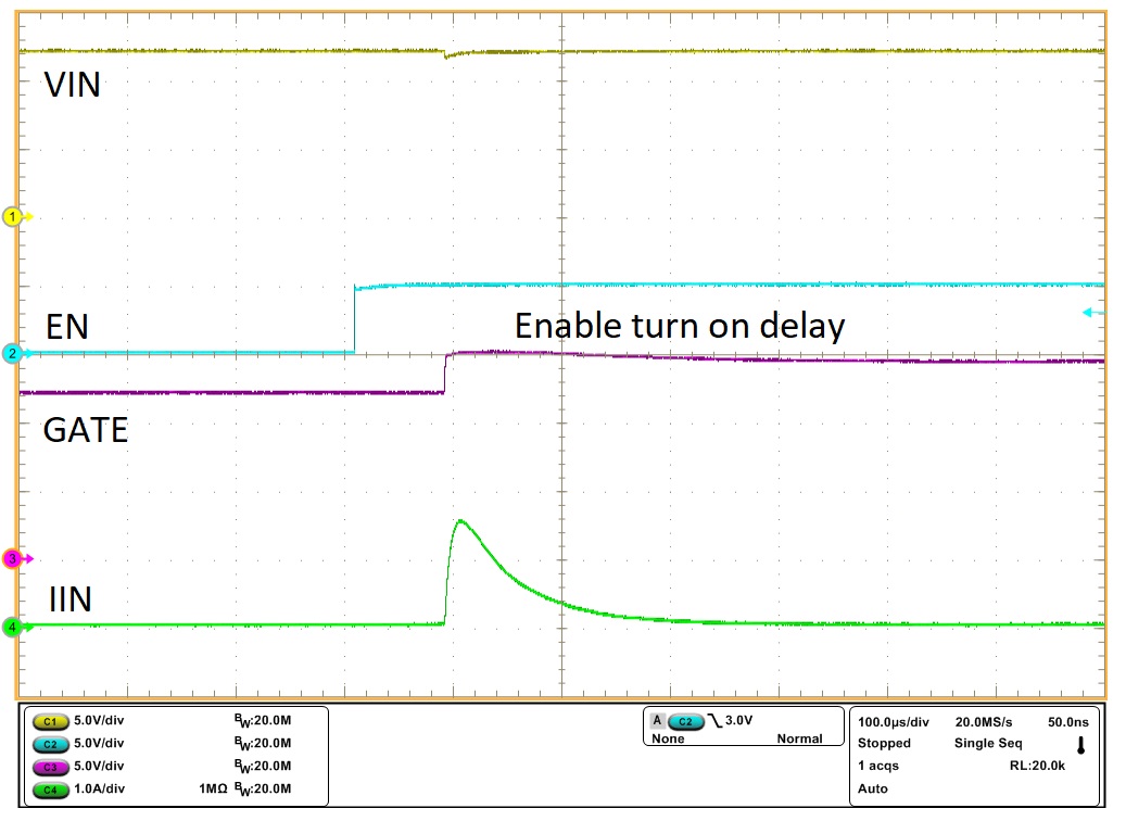
Figure 10-11 Enable Turn-ON Delay
GUID-20230814-SS0I-3W1R-9XLJ-HCBPSXKH7KNJ-low.png
Time (5 ms/DIV)
Figure 10-13 OR-ing VIN1 to VIN2 Switch Over
GUID-20230912-SS0I-0MTF-0KRT-B2GPVKPTQFGR-low.png
Time (5 ms/DIV)
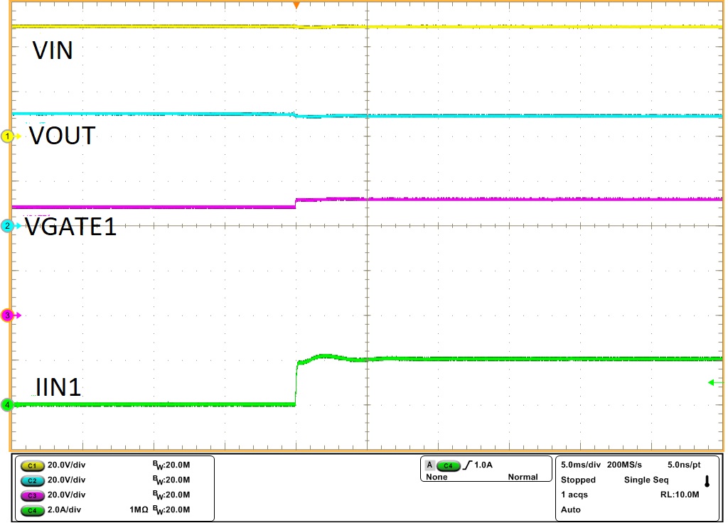
Figure 10-15 OR-ing VIN2 to VIN1 Switch Over
GUID-20230912-SS0I-JCXQ-B9LN-TPF85SCWQ509-low.jpg
Time (10 ms/DIV)
Figure 10-17 OR-ing - VIN2 Failure and Switch Over to VIN1