SNOSDB8A June   2021  – December 2021 LM74701-Q1

PRODUCTION DATA  

  1. Features
  2. Applications
  3. Description
  4. Revision History
  5. Pin Configuration and Functions
  6. Specifications
    1. 6.1 Absolute Maximum Ratings
    2. 6.2 ESD Ratings
    3. 6.3 Recommended Operating Conditions
    4. 6.4 Thermal Information
    5. 6.5 Electrical Characteristics
    6. 6.6 Switching Characteristics
    7. 6.7 Typical Characteristics
  7. Parameter Measurement Information
  8. Detailed Description
    1. 8.1 Overview
    2. 8.2 Functional Block Diagram
    3. 8.3 Feature Description
      1. 8.3.1 Input Voltage
      2. 8.3.2 Charge Pump
      3. 8.3.3 Gate Driver
      4. 8.3.4 Enable
      5. 8.3.5 Battery Voltage Monitoring (SW)
    4. 8.4 Device Functional Modes
      1. 8.4.1 Shutdown Mode
      2. 8.4.2 Conduction Mode
        1. 8.4.2.1 Regulated Conduction Mode
        2. 8.4.2.2 Full Conduction Mode
        3. 8.4.2.3 VDS Clamp Mode
      3. 8.4.3 Reverse Current Protection Mode
  9. Application and Implementation
    1. 9.1 Application Information
    2. 9.2 Typical Application
      1. 9.2.1 Design Requirements
      2. 9.2.2 Detailed Design Procedure
        1. 9.2.2.1 Design Considerations
        2. 9.2.2.2 MOSFET Selection
        3. 9.2.2.3 Charge Pump VCAP (CVCAP) and Input Capacitance (CIN)
        4. 9.2.2.4 Output Capacitance (COUT)
      3. 9.2.3 Application Curves
    3. 9.3 What to Do and What Not to Do
    4. 9.4 OR-ing Application Configuration
  10. 10Power Supply Recommendations
  11. 11Layout
    1. 11.1 Layout Guidelines
    2. 11.2 Layout Example
  12. 12Device and Documentation Support
    1. 12.1 Receiving Notification of Documentation Updates
    2. 12.2 Support Resources
    3. 12.3 Trademarks
    4. 12.4 Electrostatic Discharge Caution
    5. 12.5 Glossary
  13. 13Mechanical, Packaging, and Orderable Information

Package Options

Mechanical Data (Package|Pins)
Thermal pad, mechanical data (Package|Pins)
Orderable Information

Battery Voltage Monitoring (SW)

The LM74701-Q1 has SW pin to enable battery voltage monitoring in automotive systems. When the device is enabled, an internal switch connects SW pin to ANODE. This feature enables monitoring battery voltage using an external resistor divider connected from SW pin to GND. When LM74701-Q1 is put in shutdown mode by pulling down the EN pin low, an internal switch between SW and ANODE pin is disconnected. This action ensures there is no quiescent current drawn by the resistor ladder when system is put into low power shutdown mode. When not used, SW pin must be left floating.
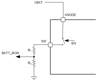
GUID-20210607-CA0I-916W-LJ1V-SZL75MPTJRBD-low.gifFigure 8-3 LM74701-Q1 SW Pin Functionality