SNOSDF7A May   2023  – December 2023 LM74703-Q1 , LM74704-Q1

PRODUCTION DATA  

  1.   1
  2. Features
  3. Applications
  4. Description
  5. Device Comparison Table
  6. Pin Configuration and Functions
  7. Specifications
    1. 6.1 Absolute Maximum Ratings
    2. 6.2 ESD Ratings
    3. 6.3 Recommended Operating Conditions
    4. 6.4 Thermal Information
    5. 6.5 Electrical Characteristics
    6. 6.6 Switching Characteristics
    7. 6.7 Typical Characteristics
  8. Parameter Measurement Information
  9. Detailed Description
    1. 8.1 Overview
    2. 8.2 Functional Block Diagram
    3. 8.3 Feature Description
      1. 8.3.1 Input Voltage
      2. 8.3.2 Charge Pump
      3. 8.3.3 Gate Driver
      4. 8.3.4 Enable
      5. 8.3.5 FET Status Indication (FETGOOD)
    4. 8.4 Device Functional Modes
      1. 8.4.1 Shutdown Mode
      2. 8.4.2 Conduction Mode
        1. 8.4.2.1 Regulated Conduction Mode
        2. 8.4.2.2 Full Conduction Mode
        3. 8.4.2.3 Reverse Current Protection Mode
  10. Application and Implementation
    1. 9.1 Application Information
    2. 9.2 Typical Application
      1. 9.2.1 Design Requirements
      2. 9.2.2 Detailed Design Procedure
        1. 9.2.2.1 Design Considerations
        2. 9.2.2.2 MOSFET Selection
        3. 9.2.2.3 Charge Pump VCAP, Input and Output Capacitance
        4. 9.2.2.4 Selection of TVS Diodes for 12-V Battery Protection Applications
        5. 9.2.2.5 Selection of TVS Diodes and MOSFET for 24-V Battery Protection Applications
      3. 9.2.3 Application Curves
    3. 9.3 Power Supply Recommendations
    4. 9.4 Layout
      1. 9.4.1 Layout Guidelines
      2. 9.4.2 Layout Example
  11. 10Device and Documentation Support
    1. 10.1 Documentation Support
      1. 10.1.1 Related Documentation
    2. 10.2 Receiving Notification of Documentation Updates
    3. 10.3 Support Resources
    4. 10.4 Trademarks
    5. 10.5 Electrostatic Discharge Caution
    6. 10.6 Glossary
  12. 11Revision History
  13. 12Mechanical, Packaging, and Orderable Information

Package Options

Mechanical Data (Package|Pins)
Thermal pad, mechanical data (Package|Pins)
Orderable Information

Application Curves

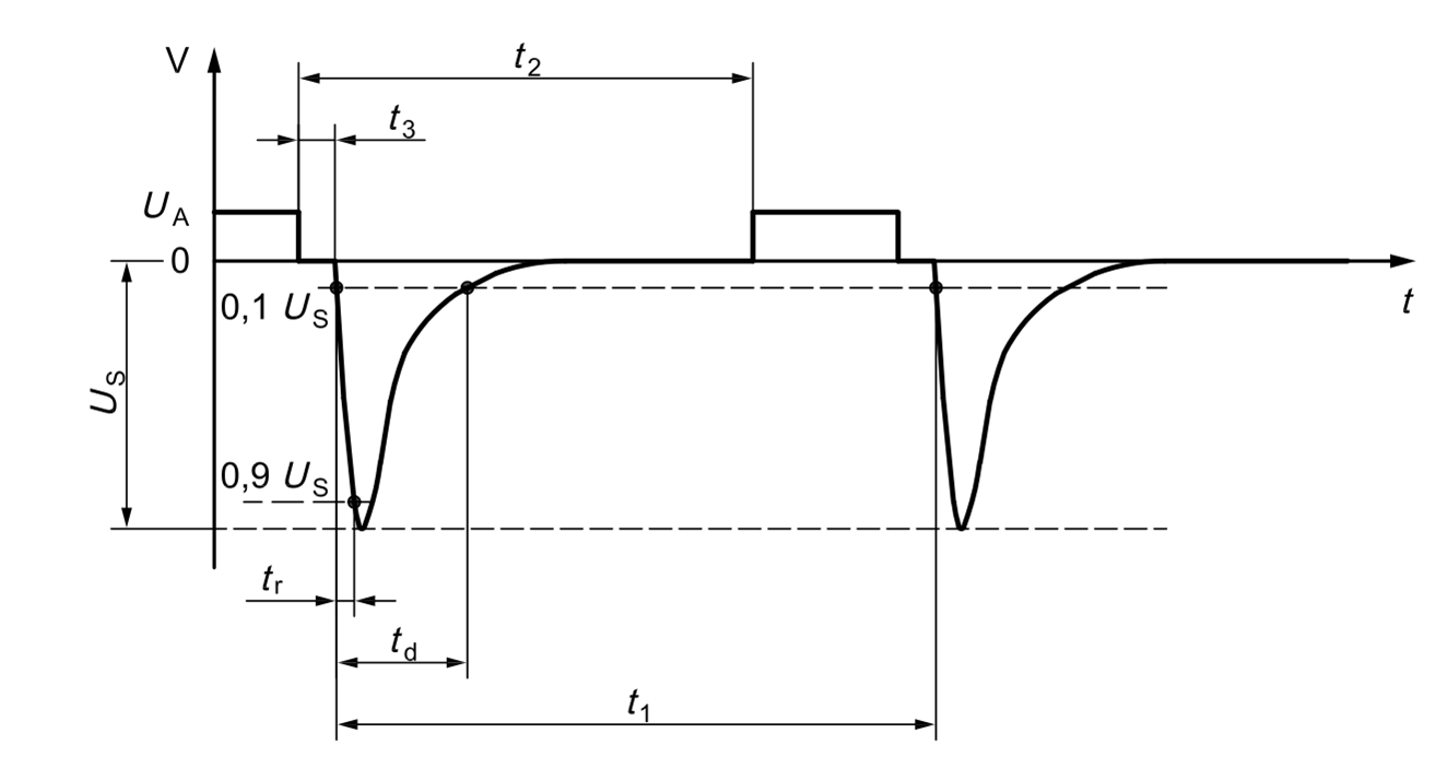
GUID-6E30A488-7C13-49CC-8E19-EF5F8E27FBDA-low.png
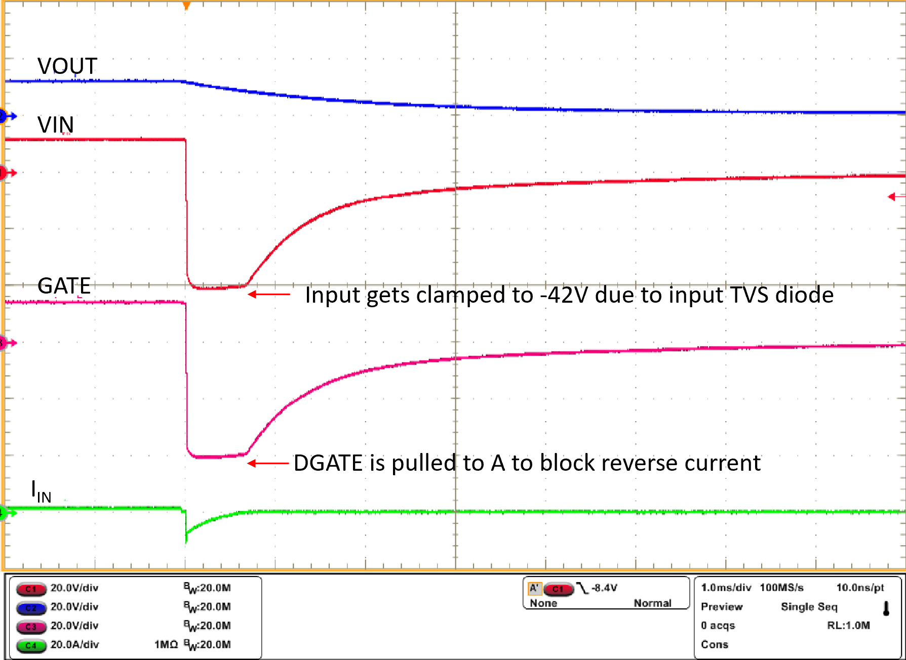
Figure 9-4 ISO 7637-2 Pulse 1
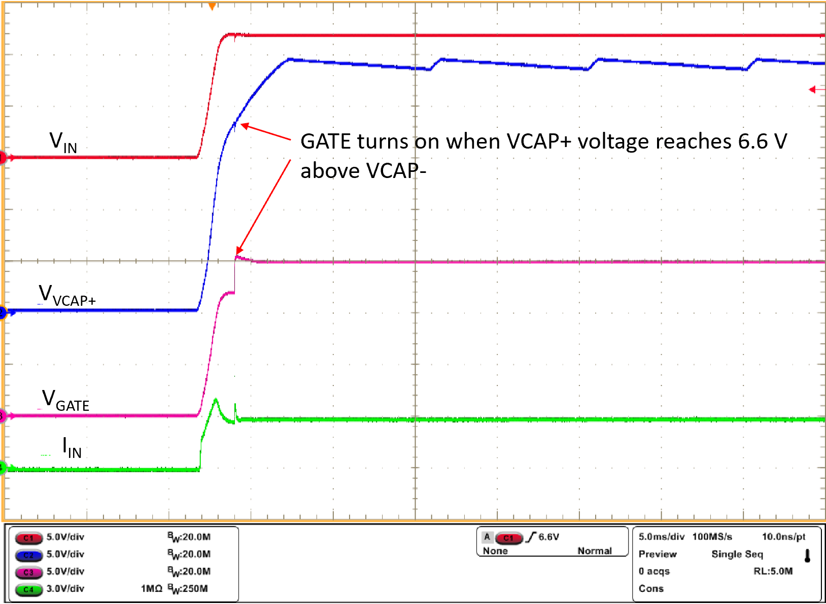
GUID-20230511-SS0I-DSSV-FMR8-3B0NVLJLVC0G-low.png
Time (5 ms/DIV)
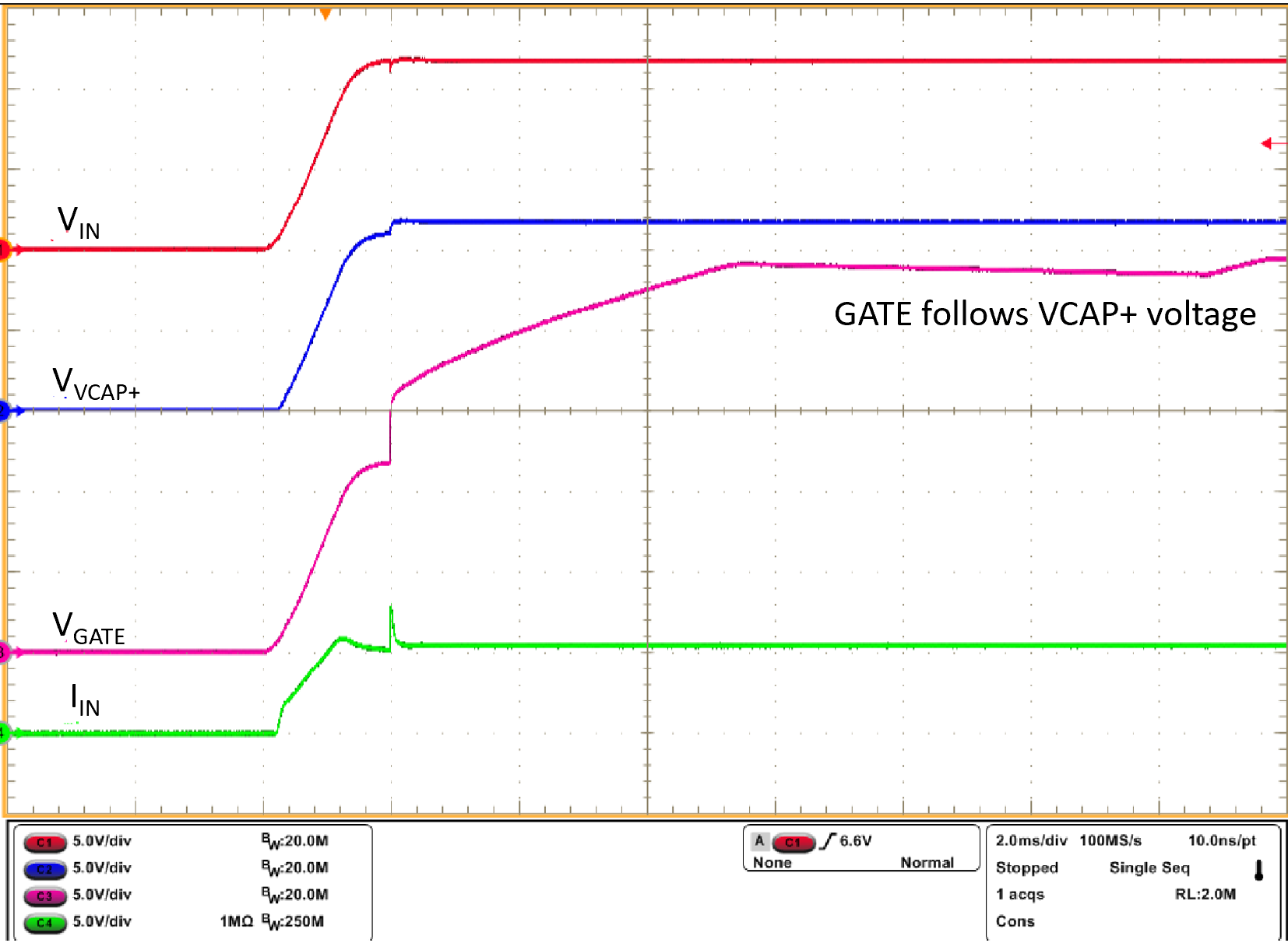
Figure 9-6 Start-up With 3-A Load
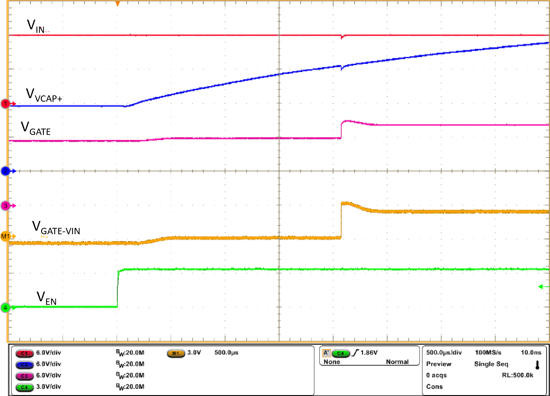
GUID-20230511-SS0I-VC4M-BCT6-1RCMNHHXS9LQ-low.png
Time (0.5 ms/DIV)
Figure 9-8 Device Start-up With EN Toggle
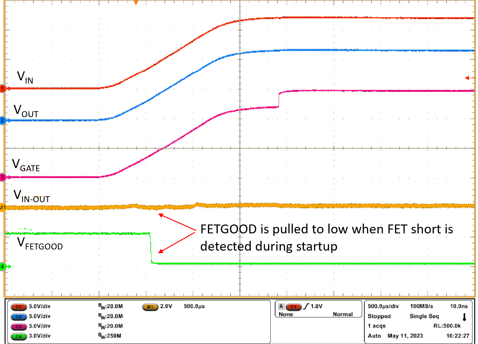
GUID-20230511-SS0I-QWDX-VTTV-WWXGMVXBJX3G-low.png
Time (0.5 ms/DIV)
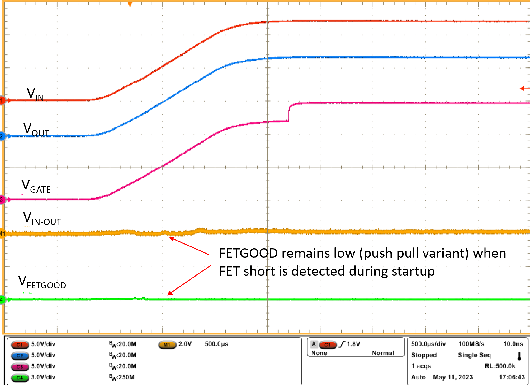
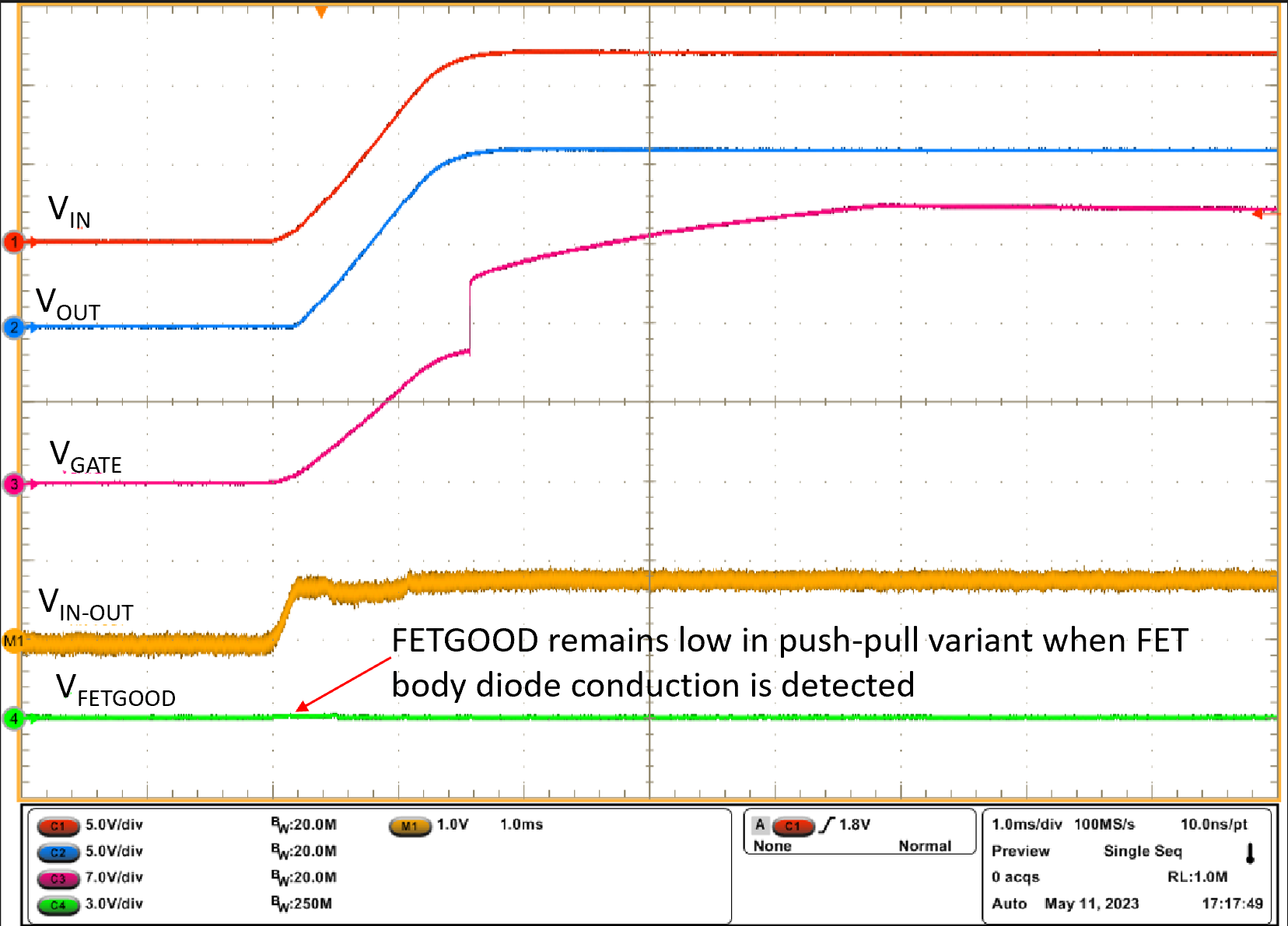
Figure 9-10 FETGOOD During Start-up With FET Short (LM74704-Q1)
GUID-20230511-SS0I-BGBR-D69W-LHT29WTVVKVM-low.png
Time (1 ms/DIV)
Figure 9-12 FETGOOD During Start-up With FET Off or GATE Pin Open (LM74704-Q1)
GUID-20230511-SS0I-3NGN-MGVQ-RZJFJGH9FK9D-low.png
Time (1 ms/DIV)
Figure 9-5 Response to ISO 7637-2 Pulse 1
GUID-20230511-SS0I-MGMW-2CW3-JHKRWHDPN2B0-low.png
Time (2 ms/DIV)
Figure 9-7 Start-up With 5.8-A Load
GUID-20230511-SS0I-XDGM-6ZDG-V9MQ8JXMG6MF-low.png
Time (0.5 ms/DIV)
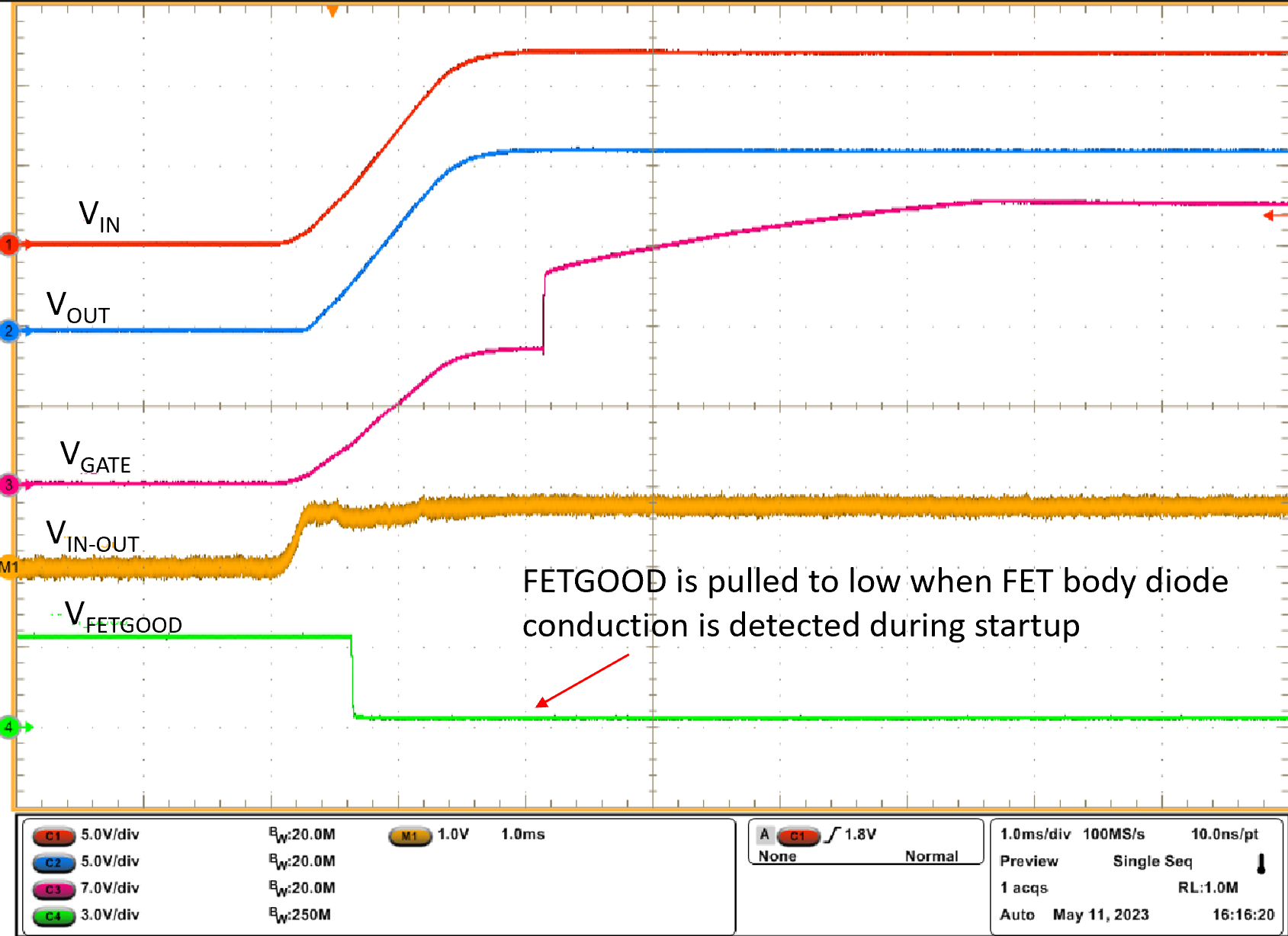
Figure 9-9 FETGOOD During Start-up With FET Short (LM74703-Q1)
GUID-20230511-SS0I-QR9D-MKZN-ZRXTTPQNSNTN-low.png
Time (1 ms/DIV)
Figure 9-11 FETGOOD During Start-up With FET Off or GATE Pin Open (LM74703-Q1)
GUID-20231127-SS0I-XVDV-4J4Z-GKZQWZF4VPQP-low.svgFigure 9-13 LM74703-Q1, LM74704-Q1 Conducted EMI Performance (150 kHz to 1 GHz)