SLVSFR9B September 2021 – August 2022 LM74722-Q1
PRODUCTION DATA
- 1 Features
- 2 Applications
- 3 Description
- 4 Revision History
- 5 Pin Configuration and Functions
- 6 Specifications
- 7 Parameter Measurement Information
- 8 Detailed Description
-
9 Application and Implementation
- 9.1 Application Information
- 9.2
Typical 12-V Reverse Battery Protection Application
- 9.2.1 Design Requirements for 12-V Battery Protection
- 9.2.2
Detailed Design Procedure
- 9.2.2.1 Design Considerations
- 9.2.2.2 Boost Converter Components (C2, C3, L1)
- 9.2.2.3 Input and Output Capacitance
- 9.2.2.4 Hold-Up Capacitance
- 9.2.2.5 Overvoltage Protection and Battery Monitor
- 9.2.2.6 MOSFET Selection: Blocking MOSFET Q1
- 9.2.2.7 MOSFET Selection: Load Disconnect MOSFET Q2
- 9.2.2.8 TVS Selection
- 9.2.3 Application Curves
- 9.3 What to Do and What Not to Do
- 10Power Supply Recommendations
- 11Layout
- 12Device and Documentation Support
- 13Mechanical, Packaging, and Orderable Information
Package Options
Mechanical Data (Package|Pins)
- DRR|12
Thermal pad, mechanical data (Package|Pins)
- DRR|12
Orderable Information
3 Description
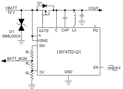
The LM74722-Q1 ideal diode controller drives and controls external back-to-back N-Channel MOSFETs to emulate an ideal diode rectifier with power path ON and OFF control and overvoltage protection. The wide input supply of 3 V to 65 V allows protection and control of 12-V and 24-V automotive battery powered ECUs. The device can withstand and protect the loads from negative supply voltages down to –65 V. An integrated ideal diode controller (GATE) drives the first MOSFET to replace a Schottky diode for reverse input protection and output voltage holdup. A strong boost regulator with fast turn-ON and OFF comparators ensures robust and efficient MOSFET switching performance during automotive testing, such as ISO16750 or LV124, where an ECU is subjected to input short interruptions and AC superimpose input signals up to 200-kHz frequency. Low quiescent current 35 µA (maximum) in operation enables always ON system designs. With a second MOSFET in the power path, the device allows load disconnect control using EN pin. Quiescent current reduces to 3.3 μA (maximum) with EN low. The device features an adjustable overvoltage cutoff or overvoltage clamp protection using OV pin.
| PART NUMBER | PACKAGE(1) | BODY SIZE (NOM) |
|---|---|---|
| LM74722-Q1 | WSON (12) | 3.00 mm × 3.00 mm |
 Low IQ Ideal Diode
 Low IQ Ideal
Diode with Switched Output