SLVSFR9B September 2021 – August 2022 LM74722-Q1
PRODUCTION DATA
- 1 Features
- 2 Applications
- 3 Description
- 4 Revision History
- 5 Pin Configuration and Functions
- 6 Specifications
- 7 Parameter Measurement Information
- 8 Detailed Description
-
9 Application and Implementation
- 9.1 Application Information
- 9.2
Typical 12-V Reverse Battery Protection Application
- 9.2.1 Design Requirements for 12-V Battery Protection
- 9.2.2
Detailed Design Procedure
- 9.2.2.1 Design Considerations
- 9.2.2.2 Boost Converter Components (C2, C3, L1)
- 9.2.2.3 Input and Output Capacitance
- 9.2.2.4 Hold-Up Capacitance
- 9.2.2.5 Overvoltage Protection and Battery Monitor
- 9.2.2.6 MOSFET Selection: Blocking MOSFET Q1
- 9.2.2.7 MOSFET Selection: Load Disconnect MOSFET Q2
- 9.2.2.8 TVS Selection
- 9.2.3 Application Curves
- 9.3 What to Do and What Not to Do
- 10Power Supply Recommendations
- 11Layout
- 12Device and Documentation Support
- 13Mechanical, Packaging, and Orderable Information
Package Options
Mechanical Data (Package|Pins)
- DRR|12
Thermal pad, mechanical data (Package|Pins)
- DRR|12
Orderable Information
8.3.1.1 Reverse Battery Protection (A, C, GATE)
A, C, GATE comprises of the ideal diode stage. Connect the source of the external MOSFET to A, drain to C and gate to GATE pin. The LM74722-Q1 has integrated reverse input protection down to –65 V.
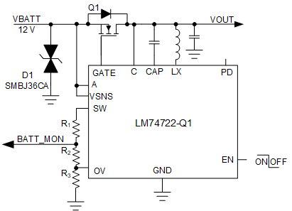
In LM74722-Q1, the voltage drop across the MOSFET is continuously monitored between the A and C pins. The GATE to A voltage is adjusted as needed to regulate the forward voltage drop at 13 mV (typical). This closed loop regulation scheme enables graceful turn-off of the MOSFET during a reverse current event and ensures zero DC reverse current flow. This scheme ensures robust performance during slow input voltage ramp down tests. Along with the linear regulation amplifier scheme, the LM74722-Q1 also integrates a fast reverse voltage comparator. When the voltage drop across A and C reaches V(AC_REV) threshold, then the GATE goes low within 0.5 µs (typical). This fast reverse voltage comparator scheme ensures robust performance during fast input voltage ramp down tests such as input micro-shorts. The external MOSFET is turned ON back when the voltage across A and C hits the V(AC_FWD) threshold within 0.72 µs (typical). As shown in Figure 8-1, for ideal diode only designs, connect LM74722-Q1.
 Figure 8-1 Configuring LM74722-Q1 for Ideal Diode Only