SNOSD95C April   2020  – December 2020 LM7480-Q1

PRODUCTION DATA  

  1. Features
  2. Applications
  3. Description
  4. Revision History
  5. Device Comparison Table
  6. Pin Configuration and Functions
  7. Specifications
    1. 7.1 Absolute Maximum Ratings
    2. 7.2 ESD Ratings
    3. 7.3 Recommended Operating Conditions
    4. 7.4 Thermal Information
    5. 7.5 Electrical Characteristics
    6. 7.6 Switching Characteristics
    7. 7.7 Typical Characteristics
  8. Parameter Measurement Information
  9. Detailed Description
    1. 9.1 Overview
    2. 9.2 Functional Block Diagram
    3. 9.3 Feature Description
      1. 9.3.1 Charge Pump
      2. 9.3.2 Dual Gate Control (DGATE, HGATE)
        1. 9.3.2.1 Reverse Battery Protection (A, C, DGATE)
        2. 9.3.2.2 Load Disconnect Switch Control (HGATE, OUT)
      3. 9.3.3 Overvoltage Protection and Battery Voltage Sensing (VSNS, SW, OV)
      4. 9.3.4 Low Iq Shutdown and Under Voltage Lockout (EN/UVLO)
    4. 9.4 Device Functional Modes
    5. 9.5 Application Examples
      1. 9.5.1 Redundant Supply OR-ing with Inrush Current Limiting, Overvoltage Protection and ON/OFF Control
      2. 9.5.2 Ideal Diode with Unsuppressed Load Dump Protection
  10. 10Applications and Implementation
    1. 10.1 Application Information
    2. 10.2 Typical 12-V Reverse Battery Protection Application
      1. 10.2.1 Design Requirements for 12-V Battery Protection
      2. 10.2.2 Automotive Reverse Battery Protection
        1. 10.2.2.1 Input Transient Protection: ISO 7637-2 Pulse 1
        2. 10.2.2.2 AC Super Imposed Input Rectification: ISO 16750-2 and LV124 E-06
        3. 10.2.2.3 Input Micro-Short Protection: LV124 E-10
      3. 10.2.3 Detailed Design Procedure
        1. 10.2.3.1 Design Considerations
        2. 10.2.3.2 Charge Pump Capacitance VCAP
        3. 10.2.3.3 Input and Output Capacitance
        4. 10.2.3.4 Hold-Up Capacitance
        5. 10.2.3.5 Overvoltage Protection and Battery Monitor
      4. 10.2.4 MOSFET Selection: Blocking MOSFET Q1
      5. 10.2.5 MOSFET Selection: Hot-Swap MOSFET Q2
      6. 10.2.6 TVS Selection
      7. 10.2.7 Application Curves
    3. 10.3 200-V Unsuppressed Load Dump Protection Application
      1. 10.3.1 Design Requirements for 200-V Unsuppressed Load Dump Protection
      2. 10.3.2 Design Procedure
        1. 10.3.2.1 Charge Pump Capacitance VCAP
        2. 10.3.2.2 Input and output capacitance
        3. 10.3.2.3 VS Capacitance, Resistor and Zener Clamp
        4. 10.3.2.4 Overvoltage Protection and Output Clamp
        5. 10.3.2.5 MOSFET Q1 Selection
        6. 10.3.2.6 Input TVS Selection
        7. 10.3.2.7 MOSFET Q2 Selection
      3. 10.3.3 Application Curves
    4. 10.4 Do's and Don'ts
  11. 11Power Supply Recommendations
    1. 11.1 Transient Protection
    2. 11.2 TVS Selection for 12-V Battery Systems
    3. 11.3 TVS Selection for 24-V Battery Systems
  12. 12Layout
    1. 12.1 Layout Guidelines
    2. 12.2 Layout Example
  13. 13Device and Documentation Support
    1. 13.1 Receiving Notification of Documentation Updates
    2. 13.2 Support Resources
    3. 13.3 Trademarks
    4. 13.4 Electrostatic Discharge Caution
    5. 13.5 Glossary
  14. 14Mechanical, Packaging, and Orderable Information

Package Options

Mechanical Data (Package|Pins)
Thermal pad, mechanical data (Package|Pins)
Orderable Information

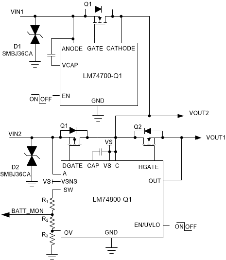
Redundant Supply OR-ing with Inrush Current Limiting, Overvoltage Protection and ON/OFF Control

GUID-050F0C2F-4016-4123-A85A-FDC07D5F0313-low.gifFigure 9-5 Redundant Supply OR-ing with Overvoltage Protection and ON/OFF Control

Figure 9-5 shows the implementation of Dual OR-ing with Inrush Current Limiting, overvoltage Protection and power path ON/OFF control. The input side SMBJ36CA TVS across the ideal diodes is required for ISO7637 Pulse 1 transient suppression to limit the input voltage within the device max voltage rating of –65V.

R1 and R2 are the programming resistors for over voltage protection (OVP) threshold. When the voltage at OV pin exceeds OV cut-off reference threshold then the HGATE driver turns OFF the FET Q3, disconnecting the power path and protecting the downstream load. HGATE goes high once the OVP pin voltage goes below the OVP falling hysteresis threshold. Use 0.1-μF to 1-μF capacitor across VS to CAP pins of the LM7480x-Q1. This is the charge pump capacitor and acts as the supply for both the DGATE and HGATE driver stages. The DGATE driver of the LM7480x-Q1 is equipped with 20-mA peak source current and 2.6-A peak sink current capability resulting in fast and efficient transient responses during the ISO16750 or LV124 short interruptions as well as AC superimpose testing.

Pull EN low during the sleep/standby mode. With EN low, both the DGATE and HGATE drivers are pulled low turning OFF both the power FETs. VOUT1 gets disconnected from the input supply rail reducing the system IQ. VOUT2 is gets power through the body diode of the MOSFET Q2 and this supply can be utilized for always ON loads. The LM7480x-Q1 draws a 2.87-μA (typ) current during this mode.