SNOSD95C April   2020  – December 2020 LM7480-Q1

PRODUCTION DATA  

  1. Features
  2. Applications
  3. Description
  4. Revision History
  5. Device Comparison Table
  6. Pin Configuration and Functions
  7. Specifications
    1. 7.1 Absolute Maximum Ratings
    2. 7.2 ESD Ratings
    3. 7.3 Recommended Operating Conditions
    4. 7.4 Thermal Information
    5. 7.5 Electrical Characteristics
    6. 7.6 Switching Characteristics
    7. 7.7 Typical Characteristics
  8. Parameter Measurement Information
  9. Detailed Description
    1. 9.1 Overview
    2. 9.2 Functional Block Diagram
    3. 9.3 Feature Description
      1. 9.3.1 Charge Pump
      2. 9.3.2 Dual Gate Control (DGATE, HGATE)
        1. 9.3.2.1 Reverse Battery Protection (A, C, DGATE)
        2. 9.3.2.2 Load Disconnect Switch Control (HGATE, OUT)
      3. 9.3.3 Overvoltage Protection and Battery Voltage Sensing (VSNS, SW, OV)
      4. 9.3.4 Low Iq Shutdown and Under Voltage Lockout (EN/UVLO)
    4. 9.4 Device Functional Modes
    5. 9.5 Application Examples
      1. 9.5.1 Redundant Supply OR-ing with Inrush Current Limiting, Overvoltage Protection and ON/OFF Control
      2. 9.5.2 Ideal Diode with Unsuppressed Load Dump Protection
  10. 10Applications and Implementation
    1. 10.1 Application Information
    2. 10.2 Typical 12-V Reverse Battery Protection Application
      1. 10.2.1 Design Requirements for 12-V Battery Protection
      2. 10.2.2 Automotive Reverse Battery Protection
        1. 10.2.2.1 Input Transient Protection: ISO 7637-2 Pulse 1
        2. 10.2.2.2 AC Super Imposed Input Rectification: ISO 16750-2 and LV124 E-06
        3. 10.2.2.3 Input Micro-Short Protection: LV124 E-10
      3. 10.2.3 Detailed Design Procedure
        1. 10.2.3.1 Design Considerations
        2. 10.2.3.2 Charge Pump Capacitance VCAP
        3. 10.2.3.3 Input and Output Capacitance
        4. 10.2.3.4 Hold-Up Capacitance
        5. 10.2.3.5 Overvoltage Protection and Battery Monitor
      4. 10.2.4 MOSFET Selection: Blocking MOSFET Q1
      5. 10.2.5 MOSFET Selection: Hot-Swap MOSFET Q2
      6. 10.2.6 TVS Selection
      7. 10.2.7 Application Curves
    3. 10.3 200-V Unsuppressed Load Dump Protection Application
      1. 10.3.1 Design Requirements for 200-V Unsuppressed Load Dump Protection
      2. 10.3.2 Design Procedure
        1. 10.3.2.1 Charge Pump Capacitance VCAP
        2. 10.3.2.2 Input and output capacitance
        3. 10.3.2.3 VS Capacitance, Resistor and Zener Clamp
        4. 10.3.2.4 Overvoltage Protection and Output Clamp
        5. 10.3.2.5 MOSFET Q1 Selection
        6. 10.3.2.6 Input TVS Selection
        7. 10.3.2.7 MOSFET Q2 Selection
      3. 10.3.3 Application Curves
    4. 10.4 Do's and Don'ts
  11. 11Power Supply Recommendations
    1. 11.1 Transient Protection
    2. 11.2 TVS Selection for 12-V Battery Systems
    3. 11.3 TVS Selection for 24-V Battery Systems
  12. 12Layout
    1. 12.1 Layout Guidelines
    2. 12.2 Layout Example
  13. 13Device and Documentation Support
    1. 13.1 Receiving Notification of Documentation Updates
    2. 13.2 Support Resources
    3. 13.3 Trademarks
    4. 13.4 Electrostatic Discharge Caution
    5. 13.5 Glossary
  14. 14Mechanical, Packaging, and Orderable Information

Package Options

Mechanical Data (Package|Pins)
Thermal pad, mechanical data (Package|Pins)
Orderable Information

Load Disconnect Switch Control (HGATE, OUT)

HGATE and OUT comprises of Load disconnect switch control stage. Connect the Source of the external MOSFET to OUT and Gate to HGATE.

Before the HGATE driver is enabled, following conditions must be achieved:

  • The EN/UVLO pin voltage must be greater than the specified input high voltage.
  • The CAP to VS voltage must be greater than the undervoltage lockout voltage.
  • Voltage at Vs pin must be greater than Vs POR Rising thershold.

If the above conditions are not achieved, then the HGATE pin is internally connected to the OUT pin, assuring that the external MOSFET is disabled.

For Inrush Current limiting, connect CdVdT capacitor and R1 as shown in Figure 9-3.
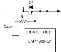
GUID-D7DDE128-28AB-4A04-8494-A3D95C63890E-low.gifFigure 9-3 Inrush Current Limiting

The CdVdT capacitor is required for slowing down the HGATE voltage ramp during power up for inrush current limiting. Use Equation 2 to calculate CdVdT capacitance value .

Equation 2. GUID-5C625847-75A2-4EFB-AC12-BA928C4F6F19-low.gif

where IHATE_DRV is 55 μA (typ), IINRUSH is the inrush current and COUT is the output load capacitance. An extra resistor, R1, in series with the CdVdT capacitor improves the turn off time.