SNOSD95C April 2020 – December 2020 LM7480-Q1
PRODUCTION DATA
- 1 Features
- 2 Applications
- 3 Description
- 4 Revision History
- 5 Device Comparison Table
- 6 Pin Configuration and Functions
- 7 Specifications
- 8 Parameter Measurement Information
- 9 Detailed Description
-
10Applications and Implementation
- 10.1 Application Information
- 10.2 Typical 12-V Reverse Battery Protection Application
- 10.3 200-V Unsuppressed Load Dump Protection Application
- 10.4 Do's and Don'ts
- 11Power Supply Recommendations
- 12Layout
- 13Device and Documentation Support
- 14Mechanical, Packaging, and Orderable Information
Package Options
Mechanical Data (Package|Pins)
- DRR|12
Thermal pad, mechanical data (Package|Pins)
- DRR|12
Orderable Information
7.7 Typical Characteristics
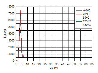 Figure 7-1 Operating Quiescent Current vs Supply
Voltage
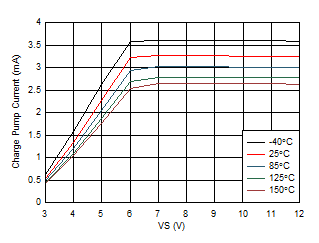 Figure 7-3 Charge Pump Current vs Supply Voltage at CAP
= 6 V
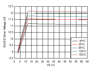 Figure 7-5 DGATE Drive Voltage vs Supply Voltage
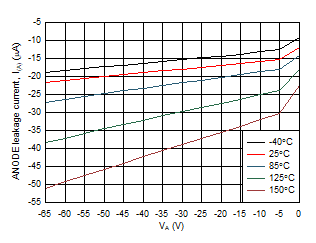 Figure 7-7 ANODE Leakage Current vs Reverse ANODE
Voltage
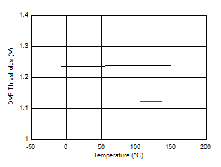 Figure 7-9 OVP Thresholds vs Temperature
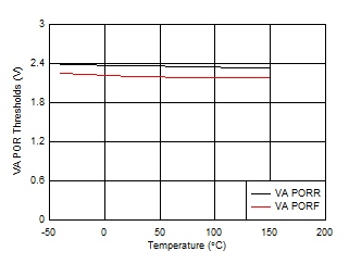 Figure 7-11 VA POR Threshold vs Temperature
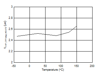 Figure 7-13 HGATE Turn OFF Delay during OV
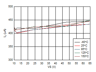 Figure 7-2 Operating Quiescent Current vs Supply
Voltage (> 10 V).
 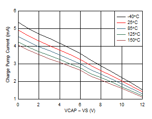 Figure 7-4 Charge Pump V-I Characteristics at VS >
= 12 V
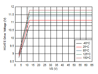 Figure 7-6 HGATE Drive Voltage vs Supply Voltage
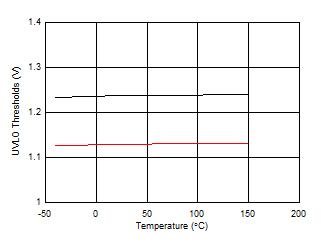 Figure 7-8 UVLO Thresholds vs Temperature
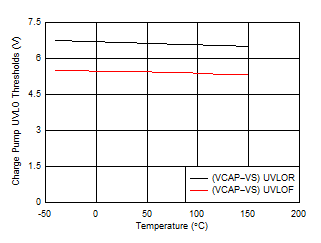 Figure 7-10 Charge Pump UVLO Threshold vs
Temperature
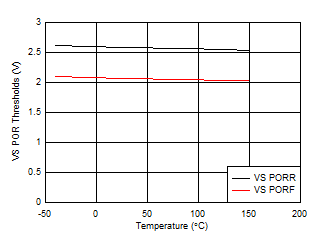 Figure 7-12 VS POR Threshold vs Temperature
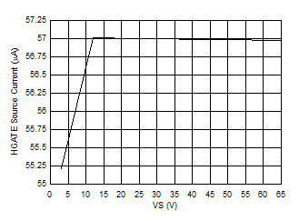 Figure 7-14 HGATE Current (IHGATE) vs Supply Voltage.