SNOSD98A May 2020 – December 2020 LM7481-Q1
PRODUCTION DATA
- 1 Features
- 2 Applications
- 3 Description
- 4 Revision History
- 5 Pin Configuration and Functions
- 6 Specifications
- 7 Parameter Measurement Information
- 8 Detailed Description
-
9 Application and Implementation
- 9.1 Application Information
- 9.2
Typical 12-V Reverse Battery Protection Application
- 9.2.1 Design Requirements for 12-V Battery Protection
- 9.2.2 Automotive Reverse Battery Protection
- 9.2.3 Input Transient Protection: ISO 7637-2 Pulse 1
- 9.2.4 AC Super Imposed Input Rectification: ISO 16750-2 and LV124 E-06
- 9.2.5 Input Micro-Short Protection: LV124 E-10
- 9.2.6 Detailed Design Procedure
- 9.2.7 MOSFET Selection: Blocking MOSFET Q1
- 9.2.8 MOSFET Selection: Hot-Swap MOSFET Q2
- 9.2.9 TVS selection
- 9.2.10 Application Curves
- 9.3 Do's and Don'ts
- 10Power Supply Recommendations
- 11Layout
- 12Device and Documentation Support
- 13Mechanical, Packaging, and Orderable Information
Package Options
Mechanical Data (Package|Pins)
- DRR|12
Thermal pad, mechanical data (Package|Pins)
- DRR|12
Orderable Information
6.7 Typical Characteristics
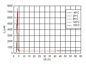
 Figure 6-1 Operating Quiescent
Current vs Supply Voltage
 Figure 6-3 Shutdown Supply Current vs Supply Voltage.
  Figure 6-5 Charge Pump V-I
Characteristics at VS > = 12 V
 Figure 6-7 HGATE Drive Voltage vs
Supply Voltage
 Figure 6-9 UVLO Thresholds vs
Temperature
 Figure 6-11 Charge Pump UVLO Threshold
vs Temperature
 Figure 6-13 VS POR Threshold vs
Temperature
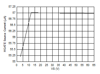
 Figure 6-15 HGATE Current (IHGATE) vs
Supply Voltage.
  Figure 6-2 Operating Quiescent
Current vs Supply Voltage (> 10 V).
  Figure 6-4 Charge Pump Current vs
Supply Voltage at CAP = 6 V
 Figure 6-6 DGATE Drive Voltage vs
Supply Voltage
 Figure 6-8 ANODE Leakage Current vs
Reverse ANODE Voltage
 Figure 6-10 OVP Thresholds vs
Temperature
 Figure 6-12 VA POR Threshold vs
Temperature
 Figure 6-14 HGATE Turn OFF Delay
during OV