SNOSD98A May 2020 – December 2020 LM7481-Q1
PRODUCTION DATA
- 1 Features
- 2 Applications
- 3 Description
- 4 Revision History
- 5 Pin Configuration and Functions
- 6 Specifications
- 7 Parameter Measurement Information
- 8 Detailed Description
-
9 Application and Implementation
- 9.1 Application Information
- 9.2
Typical 12-V Reverse Battery Protection Application
- 9.2.1 Design Requirements for 12-V Battery Protection
- 9.2.2 Automotive Reverse Battery Protection
- 9.2.3 Input Transient Protection: ISO 7637-2 Pulse 1
- 9.2.4 AC Super Imposed Input Rectification: ISO 16750-2 and LV124 E-06
- 9.2.5 Input Micro-Short Protection: LV124 E-10
- 9.2.6 Detailed Design Procedure
- 9.2.7 MOSFET Selection: Blocking MOSFET Q1
- 9.2.8 MOSFET Selection: Hot-Swap MOSFET Q2
- 9.2.9 TVS selection
- 9.2.10 Application Curves
- 9.3 Do's and Don'ts
- 10Power Supply Recommendations
- 11Layout
- 12Device and Documentation Support
- 13Mechanical, Packaging, and Orderable Information
Package Options
Mechanical Data (Package|Pins)
- DRR|12
Thermal pad, mechanical data (Package|Pins)
- DRR|12
Orderable Information
3 Description
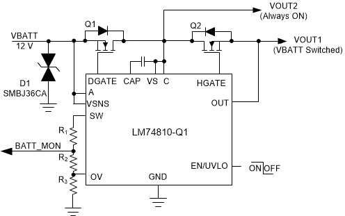
The LM74810-Q1 ideal diode controller drives and controls external back to back N-Channel MOSFETs to emulate an ideal diode rectifier with power path ON/OFF control and over voltage protection. The wide input supply of 3 V to 65 V allows protection and control of 12-V and 24-V automotive battery powered ECUs. The device can withstand and protect the loads from negative supply voltages down to –65 V. An integrated ideal diode controller (DGATE) drives the first MOSFET to replace a Schottky diode for reverse input protection and output voltage holdup. A strong charge pump of 3.8 mA with 60-mA peak GATE source current driver stage and short turn ON and turn OFF delay times ensures fast transient response ensuring robust and efficient MOSFET switching performance during automotive testing such as ISO16750 or LV124 where an ECU is subjected to input short interruptions and AC superimpose input signals upto 200-KHz frequency. With a second MOSFET in the power path the device allows load disconnect (ON/OFF control) and over voltage protection using HGATE control. The device features an adjustable over voltage cut-off protection feature for load dump protection.
| PART NUMBER | PACKAGE | BODY SIZE (NOM) |
|---|---|---|
| LM74810-Q1 | WSON (12) | 3.0 mm x 3.0 mm |
 Ideal Diode with Switched
Output
 ISO16750, LV124 AC
Superimpose Performance