SNOSDE6B december 2022 – july 2023 LM74900-Q1 , LM74910-Q1
PRODUCTION DATA
- 1
- 1 Features
- 2 Applications
- 3 Description
- 4 Revision History
- 5 Device Comparison Table
- 6 Pin Configuration and Functions
- 7 Specifications
- 8 Parameter Measurement Information
-
9 Detailed Description
- 9.1 Overview
- 9.2 Functional Block Diagram
- 9.3 Feature Description
-
10Applications and Implementation
- 10.1 Application Information
- 10.2
Typical 12-V Reverse Battery Protection Application
- 10.2.1 Design Requirements for 12-V Battery Protection
- 10.2.2 Automotive Reverse Battery Protection
- 10.2.3
Detailed Design Procedure
- 10.2.3.1 Design Considerations
- 10.2.3.2 Charge Pump Capacitance VCAP
- 10.2.3.3 Input and Output Capacitance
- 10.2.3.4 Hold-Up Capacitance
- 10.2.3.5 Selection of Current Sense Resistor, RSNS
- 10.2.3.6 Selection of Scaling Resistor (RSET) and Short-Circuit Protection Setting Resistor (RSCP)
- 10.2.3.7 Overcurrent Limit (ILIM), Circuit Breaker Timer (TMR), and Current Monitoring Output (IMON) Selection
- 10.2.3.8 Overvoltage Protection and Battery Monitor
- 10.2.4 MOSFET Selection: Blocking MOSFET Q1
- 10.2.5 MOSFET Selection: Hot-Swap MOSFET Q2
- 10.2.6 TVS Selection
- 10.2.7 Application Curves
- 10.3 Addressing Automotive Input Reverse Battery Protection Topologies With LM749x0-Q1
- 10.4 Power Supply Recommendations
- 10.5 Layout
- 11Device and Documentation Support
- 12Mechanical, Packaging, and Orderable Information
Package Options
Mechanical Data (Package|Pins)
- RGE|24
Thermal pad, mechanical data (Package|Pins)
- RGE|24
Orderable Information
3 Description
The LM749x0-Q1 ideal diode controller drives and controls external back to back N-Channel MOSFETs to emulate an ideal diode rectifier with power path ON/OFF control with overcurrent and overvoltage protection. The wide input supply of 3 V to 65 V allows protection and control of 12-V and 24-V automotive battery powered ECUs. The device can withstand and protect the loads from negative supply voltages down to –65 V. An integrated ideal diode controller (DGATE) drives the first MOSFET to replace a Schottky diode for reverse input protection and output voltage holdup. With a second MOSFET in the power path the device allows load disconnect (ON/OFF control) in case of overcurrent and overvoltage events using HGATE control. The device has integrated current sense amplifier which provides accurate current monitoring with adjustable overcurrent and short circuit thresholds. The device features an adjustable overvoltage cut-off protection feature. The device features a SLEEP mode which enables ultra-low quiescent current consumption (6 µA) and at the same time providing refresh current to the always ON loads when vehicle is in the parking state. The LM749x0-Q1 has a maximum voltage rating of 65 V.
| PART NUMBER | PACKAGE(1) | BODY SIZE (NOM) |
|---|---|---|
| LM74900-Q1 | VQFN (24) | 4.00 mm × 4.00 mm |
| LM74910-Q1 |
 Typical Application Diagram
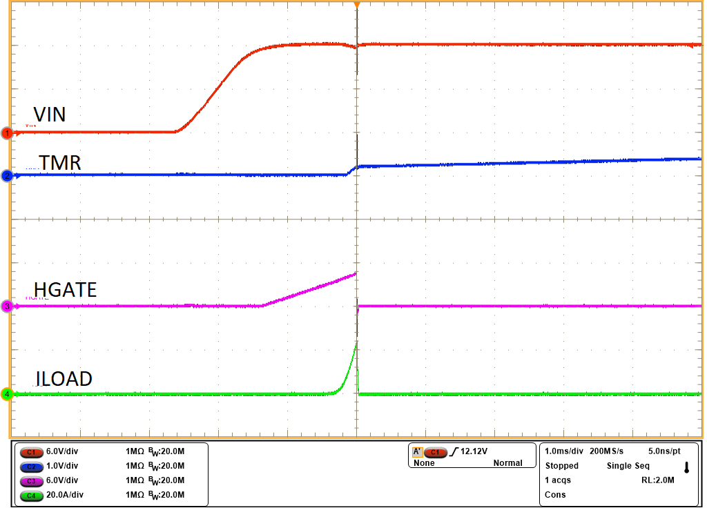
 Device Start-Up With Overcurrent Protection