SNOSDF6 October 2023 LM74930-Q1
PRODUCTION DATA
- 1
- 1 Features
- 2 Applications
- 3 Description
- 4 Revision History
- 5 Pin Configuration and Functions
- 6 Specifications
-
7 Detailed Description
- 7.1 Overview
- 7.2 Functional Block Diagram
- 7.3
Feature Description
- 7.3.1 Charge Pump
- 7.3.2 Dual Gate Control (DGATE, HGATE)
- 7.3.3 Overcurrent Protection (CS+, CS-, ILIM, IMON, TMR)
- 7.3.4 Overcurrent Protection with Circuit Breaker (ILIM, TMR)
- 7.3.5 Overcurrent Protection With Latch-Off
- 7.3.6 Short-Circuit Protection (ISCP)
- 7.3.7 Analog Current Monitor Output (IMON)
- 7.3.8 Overvoltage and Undervoltage Protection (OV, UVLO, OVCLAMP)
- 7.3.9 Disabling Reverse Current Blocking Functionality (MODE)
- 7.3.10 Device Functional Modes
-
8 Applications and Implementation
- 8.1 Application Information
- 8.2
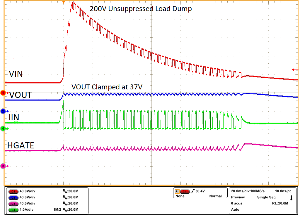
Typical Application: 200-V Unsuppressed Load Dump Protection Application
- 8.2.1 Design Requirements for 200-V Unsuppressed Load Dump Protection
- 8.2.2
Detailed Design Procedure
- 8.2.2.1 VS Capacitance, Resistor R1 and Zener Clamp (DZ)
- 8.2.2.2 Charge Pump Capacitance VCAP
- 8.2.2.3 Input and Output Capacitance
- 8.2.2.4 Overvoltage and Undervoltage Protection Component Selection
- 8.2.2.5 Selection of Scaling Resistor (RSET) and Short-Circuit Protection Setting Resistor (RSCP)
- 8.2.2.6 Overcurrent Limit (ILIM), Circuit Breaker Timer (TMR), and Current Monitoring Output (IMON) Selection
- 8.2.2.7 Selection of Current Sense Resistor, RSNS
- 8.2.2.8 Hold-Up Capacitance
- 8.2.2.9 MOSFET Q1 Selection
- 8.2.2.10 MOSFET Q2 Selection
- 8.2.2.11 Input TVS Selection
- 8.2.3 Application Curves
- 8.3 Best Design Practices
- 8.4 Power Supply Recommendations
- 8.5 Layout
- 9 Device and Documentation Support
- 10Mechanical, Packaging, and Orderable Information
Package Options
Mechanical Data (Package|Pins)
- RGE|24
Thermal pad, mechanical data (Package|Pins)
- RGE|24
Orderable Information
3 Description
The LM74930-Q1 ideal diode controller drives and controls external back to back N-Channel MOSFETs to emulate an ideal diode rectifier and power path ON and OFF control with over current and overvoltage protection. The wide input supply of 4 V to 65 V allows protection and control of 12-V and 24-V automotive battery powered ECUs. The device can withstand and protect the loads from negative supply voltages down to –65 V. An integrated high side gate control (HGATE) drives the first MOSFET in the power path. The device allows load disconnect (ON and OFF control) in case of overcurrent, overvoltage and undervoltage event using HGATE control while ideal diode controller (DGATE) drives a second MOSFET to replace a Schottky diode for input reverse polarity protection and output voltage holdup by blocking the reverse current from output to input. The device has integrated current sense amplifier which provides with an adjustable overcurrent and short circuit protection with circuit breaker functionality. The device features an adjustable overvoltage and undervoltage protection feature to protect against supply transients. LM74930-Q1 features MODE pin which can be used to selectively enable or disable reverse current blocking functionality.
 Ideal Diode With
200-V Load Dump Protection
 Unsuppressed
Load Dump 200 V - Output Clamp