SNVSAK0A October   2017  – October 2019 LM76002 , LM76003

PRODUCTION DATA.  

  1. Features
  2. Applications
  3. Description
    1.     Simplified Schematic
    2.     Efficiency vs Output Current (VOUT = 5 V, fSW = 400 kHz, Auto Mode)
  4. Revision History
  5. Pin Configuration and Functions
    1.     Pin Functions
  6. Specifications
    1. 6.1 Absolute Maximum Ratings
    2. 6.2 ESD Ratings
    3. 6.3 Recommended Operating Conditions
    4. 6.4 Thermal Information
    5. 6.5 Electrical Characteristics
    6. 6.6 Timing Characteristics
    7. 6.7 Switching Characteristics
    8. 6.8 System Characteristics
    9. 6.9 Typical Characteristics
  7. Detailed Description
    1. 7.1 Overview
    2. 7.2 Functional Block Diagram
    3. 7.3 Feature Description
      1. 7.3.1  Fixed-Frequency, Peak-Current-Mode Control
      2. 7.3.2  Light Load Operation Modes — PFM and FPWM
      3. 7.3.3  Adjustable Output Voltage
      4. 7.3.4  Enable (EN Pin) and UVLO
      5. 7.3.5  Internal LDO, VCC UVLO, and Bias Input
      6. 7.3.6  Soft Start and Voltage Tracking (SS/TRK)
      7. 7.3.7  Adjustable Switching Frequency (RT) and Frequency Synchronization
      8. 7.3.8  Minimum On-Time, Minimum Off-Time, and Frequency Foldback at Dropout Conditions
      9. 7.3.9  Internal Compensation and CFF
      10. 7.3.10 Bootstrap Voltage and VBOOT UVLO (BOOT Pin)
      11. 7.3.11 Power Good and Overvoltage Protection (PGOOD)
      12. 7.3.12 Overcurrent and Short-Circuit Protection
      13. 7.3.13 Thermal Shutdown
    4. 7.4 Device Functional Modes
      1. 7.4.1 Shutdown Mode
      2. 7.4.2 Standby Mode
      3. 7.4.3 Active Mode
      4. 7.4.4 CCM Mode
      5. 7.4.5 DCM Mode
      6. 7.4.6 Light Load Mode
      7. 7.4.7 Foldback Mode
      8. 7.4.8 Forced Pulse-Width-Modulation Mode
      9. 7.4.9 Self-Bias Mode
  8. Application and Implementation
    1. 8.1 Application Information
    2. 8.2 Typical Applications
      1. 8.2.1 Design Requirements
      2. 8.2.2 Detailed Design Procedure
        1. 8.2.2.1  Custom Design With WEBENCH® Tools
        2. 8.2.2.2  Output Voltage Setpoint
        3. 8.2.2.3  Switching Frequency
        4. 8.2.2.4  Input Capacitors
        5. 8.2.2.5  Inductor Selection
        6. 8.2.2.6  Output Capacitor Selection
        7. 8.2.2.7  Feed-Forward Capacitor
        8. 8.2.2.8  Bootstrap Capacitors
        9. 8.2.2.9  VCC Capacitors
        10. 8.2.2.10 BIAS Capacitors
        11. 8.2.2.11 Soft-Start Capacitors
        12. 8.2.2.12 Undervoltage Lockout Setpoint
        13. 8.2.2.13 PGOOD
        14. 8.2.2.14 Synchronization
      3. 8.2.3 Application Curves
  9. Power Supply Recommendations
  10. 10Layout
    1. 10.1 Layout Guidelines
      1. 10.1.1 Layout Highlights
      2. 10.1.2 Compact Layout for EMI Reduction
      3. 10.1.3 Ground Plane and Thermal Considerations
      4. 10.1.4 Feedback Resistors
    2. 10.2 Layout Example
    3. 10.3 Thermal Design
  11. 11Device and Documentation Support
    1. 11.1 Device Support
      1. 11.1.1 Development Support
        1. 11.1.1.1 Custom Design With WEBENCH® Tools
    2. 11.2 Receiving Notification of Documentation Updates
    3. 11.3 Support Resources
    4. 11.4 Trademarks
    5. 11.5 Electrostatic Discharge Caution
    6. 11.6 Glossary
  12. 12Mechanical, Packaging, and Orderable Information

Package Options

Mechanical Data (Package|Pins)
Thermal pad, mechanical data (Package|Pins)
Orderable Information

Typical Characteristics

Unless otherwise specified, VIN = 24 V. Curves represent most likely parametric norm at specified condition.
LM76002 LM76003 D001-LM76003-tc-rdson-snvsak0.gif
Figure 1. High-Side and Low-Side Switch RDS-ON
LM76002 LM76003 D003-LM76003-tc-vfb-snvsak0.gif
Figure 3. Feedback Voltage
LM76002 LM76003 D005-LM76003-tc-icl-snvsak0.gif
Figure 5. LM76002 High-Side and Low-Side Current Limits
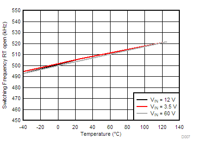
LM76002 LM76003 D007-LM76003-tc-fsw-default-snvsak0.gif
Figure 7. Switching Frequency With RT Open
LM76002 LM76003 D009-LM76003-tc-pgood-thresholds-snvsak0.gif
Figure 9. PGOOD Threshold
LM76002 LM76003 D002-LM76003-tc-ishdn-snvsak0.gif
Figure 2. Shutdown Quiescent Current
LM76002 LM76003 D004-LM76003-tc-icl-snvsak0.gif
Figure 4. LM76003 High-Side and Low-Side Current Limits
LM76002 LM76003 D006-LM76003-tc-fsw-v-rt-snvsak0.gif
Figure 6. Switching Frequency Set by RT Resistor
LM76002 LM76003 D008-LM76003-tc-en-thresholds-snvsak0.gif
Figure 8. Enable Threshold