SNVSBK6A February 2020 – July 2020 LM76005-Q1
PRODUCTION DATA
- 1 Features
- 2 Applications
- 3 Description
- 4 Revision History
- 5 Pin Configuration and Functions
- 6 Specifications
-
7 Detailed Description
- 7.1 Overview
- 7.2 Functional Block Diagram
- 7.3
Feature Description
- 7.3.1 Fixed-Frequency, Peak-Current-Mode Control
- 7.3.2 Light Load Operation Modes — PFM and FPWM
- 7.3.3 Adjustable Output Voltage
- 7.3.4 Enable (EN Pin) and UVLO
- 7.3.5 Internal LDO, VCC UVLO, and Bias Input
- 7.3.6 Soft Start and Voltage Tracking (SS/TRK)
- 7.3.7 Adjustable Switching Frequency (RT) and Frequency Synchronization
- 7.3.8 Minimum On-Time, Minimum Off-Time, and Frequency Foldback at Dropout Conditions
- 7.3.9 Bootstrap Voltage and VBOOT UVLO (BOOT Pin)
- 7.3.10 Power Good and Overvoltage Protection (PGOOD)
- 7.3.11 Overcurrent and Short-Circuit Protection
- 7.3.12 Thermal Shutdown
- 7.4 Device Functional Modes
-
8 Application and Implementation
- 8.1 Application Information
- 8.2
Typical Applications
- 8.2.1 Design Requirements
- 8.2.2
Detailed Design Procedure
- 8.2.2.1 Custom Design With WEBENCH® Tools
- 8.2.2.2 Output Voltage Setpoint
- 8.2.2.3 Switching Frequency
- 8.2.2.4 Input Capacitors
- 8.2.2.5 Inductor Selection
- 8.2.2.6 Output Capacitor Selection
- 8.2.2.7 Feedforward Capacitor
- 8.2.2.8 Bootstrap Capacitors
- 8.2.2.9 VCC Capacitors
- 8.2.2.10 BIAS Capacitors
- 8.2.2.11 Soft-Start Capacitors
- 8.2.2.12 Undervoltage Lockout Setpoint
- 8.2.2.13 PGOOD
- 8.2.2.14 Synchronization
- 8.2.3 Application Curves
- 9 Power Supply Recommendations
- 10Layout
- 11Device and Documentation Support
- 12Mechanical, Packaging, and Orderable Information
Package Options
Mechanical Data (Package|Pins)
- RNP|30
Thermal pad, mechanical data (Package|Pins)
- RNP|30
Orderable Information
7.3.6 Soft Start and Voltage Tracking (SS/TRK)
The LM76005-Q1 has a flexible and easy-to-use start-up rate control pin: SS/TRK. The soft-start feature prevents inrush current from impacting the LM76005-Q1 and its supply when power is first applied. Soft start is achieved by slowly ramping up the target regulation voltage when the device is first enabled or powered up. The simplest way to use the device is to leave the SS/TRK pin open circuit or floating. The LM76005-Q1 employs the internal soft-start control ramp and starts up to the regulated output voltage in 6.3 ms typically. In applications with a large amount of output capacitors, higher VOUT, or other special requirements, the soft-start time can be extended by connecting an external capacitor, CSS, from SS/TRK pin to AGND. Extended soft-start time further reduces the supply current required to charge up output capacitors and supply any output loading. An internal current source (ISSC = 2.2 μA) charges CSS and generates a ramp from 0 V to VFB to control the ramp-up rate of the output voltage. For a desired soft-start time tSS, the capacitance for CSS can be found by Equation 5:
where
- CSS = soft-start capacitor value (µF)
- ISSC = soft-start charging current (µA)
- tSS = desired soft-start time (s)
The soft-start capacitor CSS is discharged by an internal FET when VOUT is shut down by hiccup protection or ENABLE = logic low. When a large CSS is applied, and EN is toggled low only for a short period of time, CSS may not be fully discharged. The next soft-start ramp follows internal soft-start ramp before reaching the leftover voltage on CSS and then follows the ramp programmed by CSS. If this is not acceptable for a certain application, an R-C low-pass filter can be added to EN to slow down the shutting down of VCC, allowing more time to discharge CSS.
The LM76005-Q1 is capable of start-up into pre-biased output conditions. When the inductor current reaches zero, the LS switch is turned off to avoid negative current conduction. This operation mode is also called diode emulation mode. It is built-in by the DCM operation in light loads. With a pre-biased output voltage, the LM76005-Q1 waits until the soft-start ramp allows regulation above the pre-biased voltage and then follows the soft-start ramp to the regulation level. When an external voltage ramp is applied to the SS/TRK pin, the LM76005-Q1 FB voltage follows the ramp if the ramp magnitude is lower than the internal soft-start ramp. A resistor divider pair can be used on the external control ramp to the SS/TRK pin to program the tracking rate of the output voltage. The final voltage detected by the SS/TRK pin must not fall below 1.2 V to avoid abnormal operation.
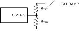
VOUT tracked to an external voltage ramp has the option of ramping up slower or faster than the internal voltage ramp. VFB always follows the lower potential of the internal voltage ramp and the voltage on the SS/TRK pin. Figure 7-4 shows resistive divider connection if external ramp tracking is desired.
 Figure 7-4 Soft-Start Tracking External Ramp
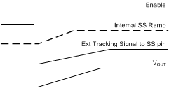
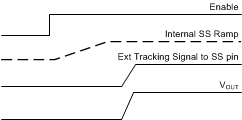
Figure 7-5 shows the case when VOUT ramps more slowly than the internal ramp, while Figure 7-6 shows when VOUT ramps faster than the internal ramp. Faster start-up time can result in inductor current tripping current protection during start-up. Use with special care.
 Figure 7-5 Tracking with Longer Start-up Time than the Internal Ramp
 Figure 7-6 Tracking with Shorter Start-up Time than the Internal Ramp
The LM76005-Q1 is capable of start-up into pre-biased output conditions. During start-up, the device sets the minimum inductor current to zero to avoid discharging a pre-biased load.