SNVSBK6A February 2020 – July 2020 LM76005-Q1
PRODUCTION DATA
- 1 Features
- 2 Applications
- 3 Description
- 4 Revision History
- 5 Pin Configuration and Functions
- 6 Specifications
-
7 Detailed Description
- 7.1 Overview
- 7.2 Functional Block Diagram
- 7.3
Feature Description
- 7.3.1 Fixed-Frequency, Peak-Current-Mode Control
- 7.3.2 Light Load Operation Modes — PFM and FPWM
- 7.3.3 Adjustable Output Voltage
- 7.3.4 Enable (EN Pin) and UVLO
- 7.3.5 Internal LDO, VCC UVLO, and Bias Input
- 7.3.6 Soft Start and Voltage Tracking (SS/TRK)
- 7.3.7 Adjustable Switching Frequency (RT) and Frequency Synchronization
- 7.3.8 Minimum On-Time, Minimum Off-Time, and Frequency Foldback at Dropout Conditions
- 7.3.9 Bootstrap Voltage and VBOOT UVLO (BOOT Pin)
- 7.3.10 Power Good and Overvoltage Protection (PGOOD)
- 7.3.11 Overcurrent and Short-Circuit Protection
- 7.3.12 Thermal Shutdown
- 7.4 Device Functional Modes
-
8 Application and Implementation
- 8.1 Application Information
- 8.2
Typical Applications
- 8.2.1 Design Requirements
- 8.2.2
Detailed Design Procedure
- 8.2.2.1 Custom Design With WEBENCH® Tools
- 8.2.2.2 Output Voltage Setpoint
- 8.2.2.3 Switching Frequency
- 8.2.2.4 Input Capacitors
- 8.2.2.5 Inductor Selection
- 8.2.2.6 Output Capacitor Selection
- 8.2.2.7 Feedforward Capacitor
- 8.2.2.8 Bootstrap Capacitors
- 8.2.2.9 VCC Capacitors
- 8.2.2.10 BIAS Capacitors
- 8.2.2.11 Soft-Start Capacitors
- 8.2.2.12 Undervoltage Lockout Setpoint
- 8.2.2.13 PGOOD
- 8.2.2.14 Synchronization
- 8.2.3 Application Curves
- 9 Power Supply Recommendations
- 10Layout
- 11Device and Documentation Support
- 12Mechanical, Packaging, and Orderable Information
Package Options
Mechanical Data (Package|Pins)
- RNP|30
Thermal pad, mechanical data (Package|Pins)
- RNP|30
Orderable Information
10.1.2 Compact Layout for EMI Reduction
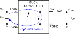
Radiated EMI is generated by the high di/dt components in pulsing currents in switching converters. The larger the area covered by the path of a pulsing current, the more electromagnetic emission is generated. The key to minimize radiated EMI is to identify the pulsing current path and minimize the area of the path. In buck converters, the pulsing current path is from the VIN side of the input capacitors to HS switch, to the LS switch, and then return to the ground of the input capacitors, as shown in Figure 10-1.
 Figure 10-1 Buck Converter High di / dt Path
High frequency ceramic bypass capacitors at the input side provide primary path for the high di/dt components of the pulsing current. Placing ceramic bypass capacitor or capacitors as close as possible to the PVIN and PGND pins is the key to EMI reduction. The SW pin connecting to the inductor must be as short as possible, and just wide enough to carry the load current without excessive heating. Short, thick traces or copper pours (shapes) must be used for high current conduction path to minimize parasitic resistance. The output capacitors must be placed close to the VOUT end of the inductor and closely grounded to PGND pin and exposed PAD. Place the bypass capacitors on VCC and BIAS pins as close as possible to the pins respectively and closely grounded to PGND and the exposed PAD.