SNVSAX6 June 2017 LM78M05-MIL
PRODUCTION DATA.
- 1 Features
- 2 Applications
- 3 Description
- 4 Revision History
- 5 Pin Configuration and Functions
- 6 Specifications
- 7 Detailed Description
- 8 Application and Implementation
- 9 Power Supply Recommendations
- 10Layout
- 11Device and Documentation Support
- 12Mechanical, Packaging, and Orderable Information
Package Options
Mechanical Data (Package|Pins)
- NDT|3
Thermal pad, mechanical data (Package|Pins)
Orderable Information
10 Layout
10.1 Layout Guidelines
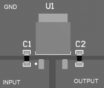
Follow these layout guidelines to ensure proper regulation of the output voltage with minimum noise. TI recommends that the input terminal be bypassed to ground with a bypass capacitor. The optimum placement is closest to the input terminal of the device and the system GND. Take care to minimize the loop area formed by the bypass-capacitor connection, the input terminal, and the system GND. Traces carrying the load current must be wide to reduce the amount of parasitic trace inductance. In cases when VIN shorts to ground, an external diode must be placed from VOUT to VIN to divert the surge current from the output capacitor and protect the device. This diode must be placed close to the corresponding device pins to increase their effectiveness.
10.2 Layout Example
 Figure 15. Layout Recommendation
10.3 Thermal Considerations
When an integrated circuit operates with appreciable current, its junction temperature is elevated. It is important to quantify its thermal limits to achieve acceptable performance and reliability. This limit is determined by summing the individual parts consisting of a series of temperature rises from the semiconductor junction to the operating environment. A one-dimension steady-state model of conduction heat transfer is demonstrated in Figure 16. The heat generated at the device junction flows through the die to the die attach pad, through the lead frame to the surrounding case material, to the printed-circuit board, and eventually to the ambient environment.
There are several variables that may affect the thermal resistance and in turn the need for a heat sink, which includes the following.
Component variables (RθJC)
- Leadframe size and material
- Number of conduction pins
- Die size
- Die attach material
- Molding compound size and material
Application variables (RθCA)
- Mounting pad size, material, and location
- Placement of mounting pad
- PCB size and material
- Traces length and width
- Adjacent heat sources
- Volume of air
- Ambient temperature
- Shape of mounting pad

The LM78M05-MIL regulator has internal thermal shutdown to protect the device from overheating. Under all possible operating conditions, the junction temperature of the device must be within the range of 0°C to 125°C. A heat sink may be required depending on the maximum power dissipation and maximum ambient temperature of the application. To determine if a heat sink is needed, the power dissipated by the regulator (PD) is calculated using Equation 1.
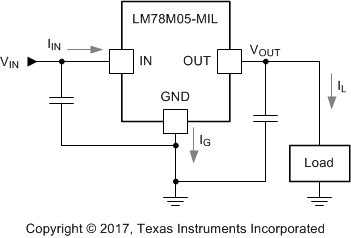
Figure 17 shows the voltages and currents which are present in the circuit.
 Figure 17. Power Dissipation Diagram
Use to calculate the maximum allowable temperature rise, TR(max).
where
- TJ(max) is the maximum allowable junction temperature (125°C)
- TA(max) is the maximum ambient temperature encountered in the application
Using the calculated values for TR(max) and PD, the maximum allowable value for the junction-to-ambient thermal resistance (RθJA) can be calculated with Equation 3.
As a design aid, Table 2 shows the value of the RθJA of TO-252 for different heat sink area. The copper patterns that we used to measure these RθJA are shown at the end of AN–1028 Maximum Power Enhancement Techniques for Power Packages (SNVA036). Figure 12 reflects the same test results as what are in the Table 2.
Figure 13 shows the maximum allowable power dissipation versus ambient temperature for the PFM device. Figure 14 shows the maximum allowable power dissipation versus copper area (in2) for the TO-252 device. For power enhancement techniques to be used with TO-252 package, see AN–1028 Maximum Power Enhancement Techniques for Power Packages (SNVA036).
Table 2. RθJA Different Heat Sink Area
| LAYOUT | COPPER AREA (in2) | THERMAL RESISTANCE: RθJA (°C/W) | |
|---|---|---|---|
| TOP SIDE(1) | BOTTOM SIDE | TO-252 | |
| 1 | 0.0123 | 0 | 103 |
| 2 | 0.066 | 0 | 87 |
| 3 | 0.3 | 0 | 60 |
| 4 | 0.53 | 0 | 54 |
| 5 | 0.76 | 0 | 52 |
| 6 | 1 | 0 | 47 |
| 7 | 0 | 0.2 | 84 |
| 8 | 0 | 0.4 | 70 |
| 9 | 0 | 0.6 | 63 |
| 10 | 0 | 0.8 | 57 |
| 11 | 0 | 1 | 57 |
| 12 | 0.066 | 0.066 | 89 |
| 13 | 0.175 | 0.175 | 72 |
| 14 | 0.284 | 0.284 | 61 |
| 15 | 0.392 | 0.392 | 55 |
| 16 | 0.5 | 0.5 | 53 |