SNIS140F May 2006 – September 2015 LM94022 , LM94022-Q1
PRODUCTION DATA.
- 1 Features
- 2 Applications
- 3 Description
- 4 Revision History
- 5 Pin Configuration and Functions
- 6 Specifications
- 7 Detailed Description
- 8 Application and Implementation
- 9 Power Supply Recommendations
- 10Layout
- 11Device and Documentation Support
- 12Mechanical, Packaging, and Orderable Information
Package Options
Mechanical Data (Package|Pins)
- DCK|5
Thermal pad, mechanical data (Package|Pins)
Orderable Information
8 Application and Implementation
NOTE
Information in the following applications sections is not part of the TI component specification, and TI does not warrant its accuracy or completeness. TI’s customers are responsible for determining suitability of components for their purposes. Customers should validate and test their design implementation to confirm system functionality.
8.1 Application Information
The LM94022/-Q1 features make it suitable for many general temperature sensing applications. It can operate over a supply range of 1.5 V to 5.5 V with programmable output slope and a wide –50°C to +150°C temperature range, thus allowing flexibility for different temperature and supply voltage range combinations.
LM94022 Transfer Function
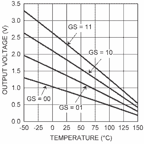
The LM94022 has four selectable gains, each of which can be selected by the GS1 and GS0 input pins. The output voltage for each gain, across the complete operating temperature range is shown in Table 2. This table is the reference from which the LM94022 accuracy specifications (listed in the Electrical Characteristics section) are determined.
Although the LM94022 transfer curves are very linear, they do have a slight umbrella parabolic shape. This shape is very accurately reflected in Table 2. The transfer table was used to calculate the following equations.

A linear approximation can be useful over a narrow temperature range. A line can easily be calculated over the desired temperature range from the table using the two-point equation:

where
- V is in mV,
- T is in °C,
- T1 and V1 are the coordinates of the lowest temperature,
- T2 and V2 are the coordinates of the highest temperature.
For example, to determine the equation of a line with the Gain Setting at GS1 = 0 and GS0 = 0, over a temperature range of 20°C to 50°C, proceed as follows:


Using this method of linear approximation, the transfer function can be approximated for one or more temperature ranges of interest. The accuracy will suffer slightly in favor of easy conversion of the output voltage to temperature.
8.2 Typical Application
8.2.1 Design Requirements
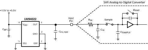
Most CMOS ADCs found in microcontrollers and ASICs have a sampled data comparator input structure. When the ADC charges the sampling cap, it requires instantaneous charge from the output of the analog source such as the LM94022/-Q1 temperature sensor and many op amps. This requirement is easily accommodated by the addition of a capacitor CFILTER).
8.2.2 Detailed Design Procedure
The size of CFILTER depends on the size of the sampling capacitor and the sampling frequency. Since not all ADCs have identical input stages, the charge requirements will vary. This general ADC application is shown as an example only.
8.2.3 Application Curve
 Figure 16. Programmable Analog Output Transfer Function
8.3 System Examples
8.3.1 Application Circuits
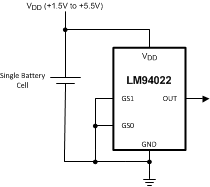
 Figure 17. Full-Range Celsius Temperature Sensor (−50°C to +150°C) Operating from a Single Battery Cell
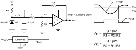
 Figure 18. Celsius Thermostat
 Figure 19. Conserving Power Dissipation With Shutdown
