SNAS487B September 2009 – March 2015 LM98722
PRODUCTION DATA.
- 1 Features
- 2 Applications
- 3 Description
- 4 Revision History
- 5 Pin Configuration and Functions
- 6 Specifications
-
7 Detailed Description
- 7.1 Overview
- 7.2 Functional Block Diagrams
- 7.3
Feature Description
- 7.3.1 Modes of Operation Introduction
- 7.3.2 Mode 3 - Three Channel Input/Synchronous Pixel Sampling
- 7.3.3 Mode 2 - Two Channel Input/Synchronous Pixel Sampling
- 7.3.4 Mode 1 - One Channel Input
- 7.3.5 CIS Lamp and Coefficient Modes
- 7.3.6 Clock Sources
- 7.3.7 Clock Sources - Additional Settings and Flexibility
- 7.3.8 Spread Spectrum Clock Generation (SSCG)
- 7.3.9 Typical EMI Cases and Recommended SSCG Settings
- 7.3.10 Recommended Master/Slave, Clock Source and SSCG Combinations and Settings
- 7.4
Device Functional Modes
- 7.4.1 Mode 3 - Three Channel Input/Synchronous Pixel Sampling
- 7.4.2 Mode 2 - Two Channel Input/Synchronous Pixel Sampling
- 7.4.3 Mode 1 - One Channel Input
- 7.4.4 Input Bias and Clamping
- 7.4.5 Sample/Hold Mode
- 7.4.6 DC Coupled Applications
- 7.4.7 Input Source Follower Buffers
- 7.4.8 CDS Mode
- 7.4.9 VCLP DAC
- 7.4.10 Gain and Offset Correction
- 7.4.11 LM98722 Typical Line Timing and Pixel Gain Regions
- 7.4.12
Automatic Black and White Level Calibration Loops
- 7.4.12.1 Calibration Overview
- 7.4.12.2 Different Modes for Different Needs
- 7.4.12.3 Calibration Initiation
- 7.4.12.4 Key Calibration Settings
- 7.4.12.5 General Black Loop Operation
- 7.4.12.6 ADAC/DDAC Convergence
- 7.4.12.7 General White Loop Operation
- 7.4.12.8 White Loop Modes
- 7.4.12.9 Bimodal (Automatic) Correction
- 7.4.13 Coarse Pixel Phase Alignment
- 7.4.14 Internal Sample Timing
- 7.4.15 CCD Timing Generator Master/Slave Modes
- 7.4.16 LVDS Control Bit Coding - LM98714 Mode
- 7.4.17 Flexible LVDS Formatting Mode: Mapping
- 7.4.18 LVDS Data Randomization for EMI Reduction
- 7.4.19 LVDS Drive Strength Adjust
- 7.4.20 LVDS Output Timing Details
- 7.4.21 LVDS Data Latency Diagrams
- 7.4.22 Data Test Patterns
- 7.4.23 CMOS Output Format
- 7.4.24 CMOS Output Data Latency Diagrams
- 7.4.25 Serial Interface
- 7.5 Registers Maps
- 8 Layout
- 9 Device and Documentation Support
- 10Mechanical, Packaging, and Orderable Information
Package Options
Mechanical Data (Package|Pins)
- DGG|56
Thermal pad, mechanical data (Package|Pins)
Orderable Information
7 Detailed Description
7.1 Overview
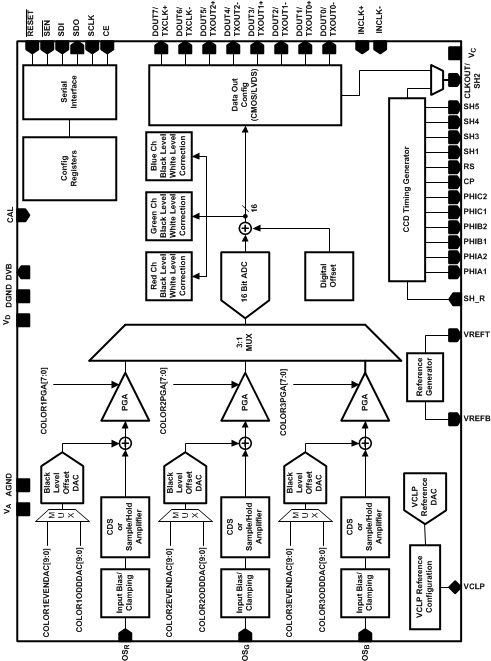
The LM98722 is a 16-bit, three-input, complete Analog Front End (AFE) for digital color copier and Multi-Function Peripheral (MFP) applications. The system block diagram of the LM98722, shown in LM98722 Overall Chip Block Diagram highlights the main features of the device. Each input has its own Input Bias and Clamping Network which are routed through a selectable Sample/Hold (S/H) or Correlated Double Sampler (CDS) amplifier. A +/-9-Bit Offset DAC applies independent offset correction for each channel. A -3 to 17.9dB Programmable Gain Amplifier (PGA) applies independent gain correction for each channel. The LM98722 also provides independent Digital Black Level Correction Feedback Loops for each channel. The Black Level Correction Loop can be configured to run in Manual Mode (where the user inputs their own values of DAC offset) or in Automatic Mode where the LM98722 calculates each channel’s Offset DAC value during optical black pixels and then adjusts the Offset register accordingly. The signals are routed to a single high performance 16-bit, 45-MHz analog-to-digital converter.
The analog inputs are protected as shown in Figure 1. Input voltage magnitude up to 500 mV beyond the supply rails will not damage this device. However, input errors will be generated if the input goes above VA and below AGND.
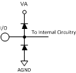 Figure 1.
7.2 Functional Block Diagrams
7.2.1 LM98722 Overall Chip Block Diagram
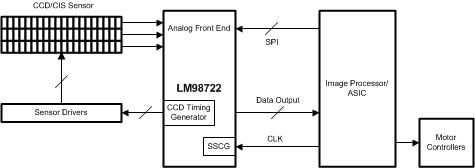
7.2.2 System Block Diagram
7.3 Feature Description
7.3.1 Modes of Operation Introduction
The LM98722 can be configured to operate in several different operating modes. The following sections are a brief introduction to these modes of operation. A more rigorous explanation of the operating modes is contained in Device Functional Modes, including input sampling diagrams for each mode as well as a description of the operating conditions.
7.3.2 Mode 3 - Three Channel Input/Synchronous Pixel Sampling
OSB, OSG, and OSR inputs are sampled synchronously at a pixel rate. The sampled signals are processed with each channel’s offset and gain adjusted independently via the control registers. The order in which pixels are processed from the input to the ADC is fully programmable and is synchronized by the SH pulse. In this mode, the maximum channel speed is 15MSPS per channel with the ADC running at 45MSPS yielding a three color throughput of 45MSPS.
7.3.3 Mode 2 - Two Channel Input/Synchronous Pixel Sampling
Mode 2 is useful for CCD sensors with a Black and White mode with Even and Odd outputs. In its default configuration, Mode 2 samples the Even output via the OSB channel input, and the Odd output via the OSG channel input. Sampling of the Even and Odd pixels is performed synchronously at a maximum sample rate of 22.5MSPS per input with the ADC running at 45MSPS
7.3.4 Mode 1 - One Channel Input
In Mode 1, all pixels are processed through a single input (OSR, OSG, or OSB) chosen through the control register setup. This mode is useful in applications where only one input channel is used. The selected input is programmable through the control register.
7.3.5 CIS Lamp and Coefficient Modes
In additional to Modes 3, 2, and 1 above, two different CIS sensor modes (CISa and CISb) can be enabled. These allow color sequential lamp control, as well as synchronized color sequential gain/offset coefficient usage for multi-output color sequential sensors.
7.3.6 Clock Sources
7.3.6.1 User Provided Clock Signal
When XTALEN = 0 (Page 0, Register 0, Bit 2) the clock input to the LM98722 can be a differential LVDS clock on the INCLK+ and INCLK- pins or a CMOS level clock applied to the INCLK+ pin with the INCLK- pin connected to DGND. The external clock signal format is auto sensed internally.
7.3.6.2 Crystal Oscillator Driver On-Chip
When XTALEN = 1 (Page 0, Register 0, Bit 2), an on-chip crystal oscillator driver circuit can be paired with an external crystal. Terminal 2 of the crystal should connect to INCLK+ and terminal 1 of the crystal should connect to INCLK-. 18 pF capacitors should connect from each terminal of the crystal to ground.
7.3.6.3 Clock Multiplication - Basic
For any of the available clock sources, the input clock can be applied at the Pixel frequency (PIXCLK) or at the ADC frequency (ADCCLK). The LM98722 can perform internal clock multiplication when a Pixel frequency clock is applied, or no multiplication when an ADC frequency clock is applied. The internal configuration registers need to be written to perform the proper setup of the input clock. The available input clock configurations for each operating mode is outlined in Table 1.
Table 1. Input Clock Configurations for Operating Modes
| AFE MODE | INPUT CLOCK TYPE | INTERNAL MULTIPLIER | INCLK MAX FREQ. | CONFIGURATION REGISTER SETTINGS |
|---|---|---|---|---|
| Mode 3 | INCLK = Pixel Freq. (PIXCLK) | 3x | 15 MHz | TBD |
| INCLK = ADC Freq. (ADCCLK) | 1x | 45 MHz | TBD | |
| Mode 2 | INCLK = Pixel Freq. (PIXCLK) | 2x | 22.5 MHz | TBD |
| INCLK = ADC Freq. (ADCCLK) | 1x | 45 MHz | TBD | |
| Mode 1 | INCLK = Pixel Freq. = ADC Freq | 1x | 22.5 MHz | TBD |
| (ADCCLK = PIXCLK in Mode 1) |
7.3.6.4 Clock Multiplication - Flexible
There are a variety of situations where it is desirable to multiply the base frequency by a selected amount to achieve the proper pixel frequency for a given application and set of system conditions.
- Applications using the onchip Crystal Oscillator driver will have much more flexibility of pixel frequencies.
- Reducing the input MCLK frequency can significantly reduce the EMI generated by the MCLK signals being sent up the cable from the host board to the imaging board.
To ease this task a flexible multiplying PLL architecture is incorporated. When the 2 PLL architecture is enabled (Page 2, Register 0x1Bh, Bit 1=0) the source clock frequency is multiplied by the ratio M/N. Two registers are used to set these values:
- M = Value(Page 2, Register 0x1Ch) + 1
- N = Value(Page 2, Register 0x1Dh) + 1
- N(max) = 64
- M/N(max) = 64
- M/N(min) = 1/64
- Note: Since the 8 bit register values can be from 0 to 255, the resulting Numerator and Denominator values could be from 1 to 256. However, the maximum recommended multiply or divide ratios are 64x or x/64. In addition, the maximum recommended value for N is 64.
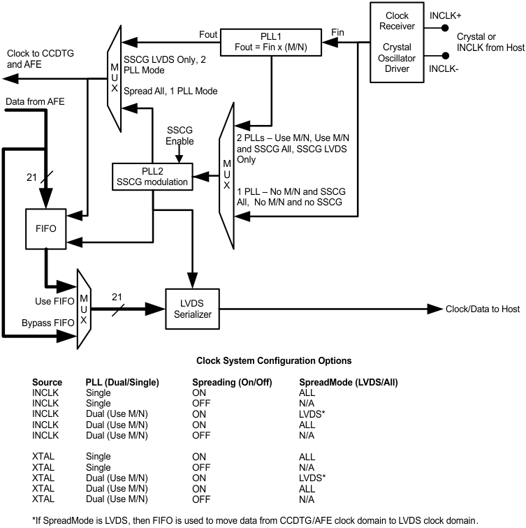 Figure 2. Clock System Block Diagram
7.3.7 Clock Sources - Additional Settings and Flexibility
To support the new crystal oscillator feature, some additional flexibility was added. In Crystal Oscillator mode, the master clock source is now on the AFE (rather than in the system ASIC or main processor). If Slave Timing Mode (see Device Functional Modes) is still needed (to synchronize the AFE to the line timing of the system), the external SH_R signal must now be captured with the internal clock source. The SH_R Capture Clock Select bit has been added to support this case.
In addition, in these systems, it may be difficult to adjust the host SH_R timing to get the best Setup and Hold times with respect to the internal CLK. The SH_R, INCLK Monitor Override and SH_R Capture Edge Select controls have been added to support these needs. The INCLK Monitor Override allows the internal SH_R and CLK signals to be monitored, to aid in selected the best edge (rising or falling) of CLK to latch the SH_R signal.
- SH_R Capture Clock Select (Page 0, Register 0x00, Bit 5)
- SH_R Capture Edge Select (Page 0, Register 0x00, Bit 4)
- 0 - Use rising edge of selected clock source
- 1 - Use falling edge of selected clock source
- SH_R and INCLK Monitor Override (Page 0, Register 0x14, Bit 6)
- 0 - Timing monitor selections unaltered
- 1 - Timing monitors for CLAMPB and SAMPB are replaced with monitor of SH_R_Internal and SH_R Capture_Clock_Internal.
7.3.8 Spread Spectrum Clock Generation (SSCG)
NOTE
When using SSCG, ensure that INCLK = ADCCLK is selected at Page 0, Register 0x02, Bit 2 = 0. Then set the flexible clock multiplication PLL settings to achieve the desired internal clock frequency from the applied clock.
EMI is a problem faced by any system designer. In a typical imaging system, data must be sent over a relatively long cable to the main system board. To minimize the amount of measured EMI caused by system clocking and data transmission, a flexible Spread Spectrum Clock Generation system is included in the LM98722.
The spread spectrum feature is configured by the registers at Page 2, Registers 0x1Ah, 0x1Bh and 0x1Eh.
The following key SSCG modes of operation and features are provided:
- Spread output data/clock only (Internal FIFO used to transfer data between clock domains) or spread internal system clock as well as output data/clock
- Spread synchronized to CCD line length (SH period or frequency) or unsychronized.
- Spread widths of 0.625, 1.25, 2.5 and 5% selectable
- Spread gain of 1x to 2x can double the selected spread widths
- 3 selectable modulation frequency multipliers to increase the spreading modulation frequency
- Spread “boost” provides a cleaner spread for 1 channel and 2 channel modes of AFE operation
- Spread MaxRate allows the most effective spreading modulation for Output Only spreading. When this bit is set, the spreading waveform is NOT synchronized to the CCD line timing.
- Spreading modulation waveform and FIFO reset by SH_R event. (Page 8, Register 0x1Eh, Bit 7) This ensures that the spread- ing waveform is synchronized to the CCD line timing, even if SH_R to SH_R period is varied by system ASIC.
- Spreading SH_R Reset can be delayed from SH_R event by a “Holldoff” amount. (Page 8, Register 0x1Eh, Bits6:0)
7.3.9 Typical EMI Cases and Recommended SSCG Settings
Case 1: Majority of EMI coming from LVDS outputs
Usage: Spread output data/clock only. FIFO used to move data between non-spread and spread clock domains. If Slave Mode is also used, ensure that the Line Length and Line Length Multiplier settings correspond to the SH_R period. If the SH_R period may vary, then set FIFO Reset (Page 2, Register 0x1Bh, Bit 6 =1) to ensure the FIFO counters are reset every SH Interval.
Case 2: EMI from LVDS outputs and CCD timing signals - Master Mode Application
Usage: Spread internal system clock as well as output data/clock. Synchronize spread waveform to SH Interval. Best to use Master mode timing to ensure spread waveform is always smoothly synchronized to the SH Interval timing.
Case 3: EMI from LVDS outputs and CCD timing signals - Slave Mode Application
Usage: Spread internal system clock as well as output data/clock. Use minimal amount of spreading to reduce CCD timing emissions, in combination with data scrambling to further reduce data cable emissions. The small amount of spreading minimizes effects on image data, therefore, spreading is not required to be synchronized with SH Intervals.
7.3.10 Recommended Master/Slave, Clock Source and SSCG Combinations and Settings
7.3.10.1 Master Mode Operation (LM98722 Controls Line Timing)
(These are easiest cases to implement SSCG)
Clock From Host Board
- Use SSCG - Spread All
- Use SSCG - Spread LVDS Only
- No SSCG
Clock From Local Crystal
- Use SSCG - Spread All
- Use SSCG - Spread LVDS Only
- No SSCG
7.3.10.2 Slave Mode Operation (Host FPGA or ASIC Controls Line Timing)
(These SSCG cases are more challenging as received LVDS data timing will not be synchronous with the clock of the FPGA/ASIC. Clock from host board. If a local clock is present on the FPGA/ASIC, an internal FIFO must be implemented to transfer the received data from the spread LVDS clock domain, to the internal FPGA/ASIC clock domain. If the AFE LVDS clock is used as the system clock, care must be taken to ensure that settings are not loaded which disable this clock, and therefore lock up the system.)
- Use SSCG - Spread All - Need spreading start to be SH gated, and SH period to be consistent to ensure consistent capture of SH_R by the spread INCLK.
- Use SSCG - Spread LVDS Only - In this case ensure that Line Length Register is set to same number of pixels as that or SH_R period. In addition, if SH_R period will vary, set FIFO Reset (Page 2, Register 0x1Bh, Bit 6 = 1) to reset FIFO at SH Interval.
- No SSCG
Clock from local crystal (Not recommended, difficult to meet CLK to SH_R setup and hold times. Use Master Mode instead)
- Use SSCG - Spread All
- Use SSCG - Spread LVDS Only
- No SSCG
7.3.10.3 SSCG Configuration/Usage Flow
- Unlock Registers (Page 0, Register 0, Bit 0 = 0)
- Ensure PIXCLK/ADCCLK Configuration is set to ADCCLK. Page 0, Register 0x02, Bit 2 = 0.
- Set Override PLL2 Lock Detector (Page 2, Register 0x1B, Bit 4) = 1
- Set PLL2 Charge Pump Current Control (Page 2, Register 0x19, Bits 4:3) = 00
- Set PLL2 Filter Bandwidth Control (Page 2, Register 0x19, Bits 2:0) = 111
- Set SSCG Spread Boost (Page 2, Register 0x1A, Bit 5) = 0 or 1 (0 = default, recommended for most applications)
- Set SSCG Spread Gain (Page 2, Register 0x1A, Bit 4) = 0 or 1 (0 = default, recommended for most applications)
- Set SSCG Spread Width (Page 2, Register 0x1A, Bits 3:2) = 0.625% to 2.5% (Beyond 2.5% most LVDS deserializers will not track the clock properly)
- Set SSCG SH Sync Enable (Page 2, Register 0x1A, Bit 1) = 0 or 1 (Set to 1 for Spread All)
- Set PLL Mode Select (Page 2, Register 0x1B, Bits 1:0) = 00, 01 or 11. Spread Output Only or Spread All Clocks
- If PLL Clock Multiplication Enabled, Set Clock Mult M (Page 2, Register 0x1C) and N (Page 2, Register 0x1D) to desired values. If a pixel rate clock is applied, set the PLL multiplication to the same factor as the AFE Mode selected at Page 0, Register 0x03, Bits 7:6. ie. The multiplication factor should be 3x for Mode 3, 2x for Mode 2 and 1x for Mode 1.
- Set SSCG Enable (Page 2, Register 0x1A, Bit 0) = 1 (enable spreading, load spreading state machines)
- Lock Registers (Page 0, Register 0, Bit 0 = 1)
- If spreading is synchronized to SH interval, the spreading function will wait until the next SH Interval before beginning.
7.3.10.4 Changing SSCG Settings
To change SSCG settings:
- Un-Lock Registers ((Page 0, Register 0, Bit 0 = 0)
- Set SSCG Enable = 0 (disable spreading)
- Change desired SSCG settings.
- Set SSCG Enable = 1 (enable spreading, reload spreading state machines)
- Lock Registers (Page 0, Register 0, Bit 0 = 1)
Table 2. SSCG and Clock Multiplication Register Settings
| PAGE | REGISTER | DEFAULT | BITS | NAME | DESCRIPTION | |
|---|---|---|---|---|---|---|
| 2 | 24 | 18 | 1111 1000 | [7:5] | PLL Control 1 | Master PLL Range Setting for PLL1 and PLL2 when |
| Autorange is off. Set to 111. | ||||||
| [4:3] | PLL1 Charge Pump Current Control | |||||
| Default = 11 | ||||||
| [2:0] | PLL1 Filter Bandwidth Control | |||||
| Default = 000 | ||||||
| 2 | 25 | 19 | 0001 1000 | [7:5] | PLL Control 2 | Reserved |
| Default = 000 | ||||||
| [4:3] | PLL2 Charge Pump Current Control | |||||
| Default = 11 | ||||||
| Set to 00 when using SSCG. | ||||||
| [2:0] | PLL2 Filter Bandwidth Control | |||||
| Default = 000 | ||||||
| Set to 111 when using SSCG. | ||||||
| 2 | 26 | 1A | 0000 0000 | [7:6] | SSCG Control 1 | Spread Rate Multiplier |
| (Increases modulation frequency in low pixel frequency applications) | ||||||
| 00 1x - Default | ||||||
| 01 2x | ||||||
| 10 4x | ||||||
| 11 Reserved | ||||||
| [5] | SSCG Spread Boost | |||||
| 0 Normal, PLL divide step is 1/28 | ||||||
| 1 Boost, PLL divide step is 1/56. Narrower and cleaner spread for 1ch and 2ch modes, but limits max pixel freq to 25 MHz. | ||||||
| [4] | SSCG Spread Gain | |||||
| 0 Spread widths as specified in [3:2] | ||||||
| 1 Spread widths are 2x [3:2] settings | ||||||
| [3:2] | SSCG Spread Width (Fmod = Fcenter+/- Width/2) | |||||
| 00 5% | ||||||
| 01 2.5% | ||||||
| 10 1.25% | ||||||
| 11 0.625% | ||||||
| [1] | SSCG SH Sync Enable | |||||
| 0 Spread unsynched, once SSCG Enable and Register Lock Control are set, SSCG will begin immediately. | ||||||
| 1 Spread synched to SH interval, once SSCG Enable is set, the SSCG will begin at the first SH Interval. | ||||||
| [0] | SSCG Enable | |||||
| 0 Spread off | ||||||
| 1 Spread on | ||||||
| 2 | 27 | 1B | 0000 0010 | [7] | SSCG Control 2 | Load SSCG state machine |
| (SSCG Enable 0->1 also performs this function) | ||||||
| 0 Normal | ||||||
| 1 Load state machine (self clearing) | ||||||
| [6] | FIFO Reset at SH_R | |||||
| 0 FIFO is only reset when SSCG started | ||||||
| 1 FIFO is reset at SH_R. Only useful in Slave Mode with Spread LVDS Only set. Ensures that FIFO counters are centered if SH_R period is consistenly shorter or longer than Line Length settings. | ||||||
| [5] | Spread Waveform Reset at SH_R | |||||
| 0 Spread waveform not reset by SH_R | ||||||
| 1 Spread waveform reset by SH_R | ||||||
| [4] | Override PLL2 Lock Detector | |||||
| 0 PLL2 Lock Detector Normal | ||||||
| 1 Force PLL2 Lock Detect = 1. Set to 1 when using SSCG. | ||||||
| [3] | Override PLL1 Lock Detector | |||||
| 0 PLL1 Lock Detector Normal | ||||||
| 1 Force PLL1 Lock Detect = 1. Useful only if using a large multiplication factor and a lot of jitter is present in the source clock. | ||||||
| [2] | Spread MaxRate | |||||
| 0 Spread Normal | ||||||
| 1 Force Spreading to highest modulation frequency instead of tied to Line Length Setting. | ||||||
| [1:0] | PLL Mode Select | |||||
| 11 Spread All System Clocks, No Multiplication | ||||||
| 10 PLLs and SSCG Disabled - Default | ||||||
| 01 Spread All System Clocks, Multiplication Enabled | ||||||
| 00 Spread Output Clocks Only, Mutiplication Enabled | ||||||
| 2 | 28 | 1C | 0000 0000 | Clock Mult M | Multiplying PLL. Fout = Fin x M/N M = mmmmmmmm + 1 (1 to 256) | |
| 2 | 29 | 1D | 0000 0000 | Clock Mult N | Multiplying PLL. Fout = Fin x M/N N = nnnnnnnn + 1 (1 to 256) | |
| 2 | 30 | 1E | 0000 0000 | [7] | SSCG Control 3 | FIFO Reset |
| 0 FIFO normal operating | ||||||
| 1 Force reset of FIFO (self clearing) | ||||||
| [6:0] | FIFO and Spread Waveform SH_R Reset Holdoff | |||||
| Delay reset of FIFO and Spread Waveform from 0 to | ||||||
| 127 ADC clock cycles after the internal synchronized SH_R. To allow this event to occur during SH Interval after all valid pixels in the pipeline have been pro- cessed. |
7.4 Device Functional Modes
7.4.1 Mode 3 - Three Channel Input/Synchronous Pixel Sampling
In Mode 3, the OSR, OSG, and OSB input channels are sampled synchronously. The sampled input signals are then processed in parallel through their respective channels with each channel offset and gain adjusted by their respective control registers. The signals are then routed through a 3-1 MUX to the ADC. The order in which pixels are processed through the MUX to the ADC is programmable (OSR-OSG-OSB, or OSB-OSG-OSR) and is synchronized by the SH pulse.
Table 3. Mode 3 Operating Details
| DETAIL | |||
|---|---|---|---|
| Channels Active | OSB & OSG & OSR | 3 channel synchronous pixel sampling. | |
| Channel Sample Rate | 15 | MSPS per Channel (max) | |
| ADC Sample Rate | 45 | MSPS (max) | |
| fADC: fINCLK | Internal 3x Clock Selected | 3:1 | fINCLK = 25 MHz (max) |
| Internal 1x Clock Selected | 1:1 | fINCLK = 75 MHz (max) | |
| Output Sequencing | SH Signal --> R-G-B-R-G-B-R-G-B→ or SH Signal --> B-G-R-B-G-R-B-G-R→ |
||
7.4.2 Mode 2 - Two Channel Input/Synchronous Pixel Sampling
Mode 2 is useful for CCD sensors with a Black and White line with Even and Odd pixels. In its default configuration, Mode 2 samples Even sensor pixels via the Blue Channel Input, and Odd sensor pixels via the Green Channel Input. The selection of Even/Odd inputs can be changed through the serial interface registers. Sampling of the Even and Odd inputs is performed synchronously.
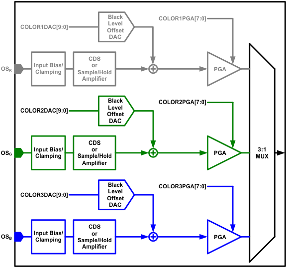 Figure 4. Mode 2 Signal Routing
Table 4. Mode 2 Operating Details
7.4.3 Mode 1 - One Channel Input
In Mode 1a, all pixels are processed through a single input (OSR, OSG, or OSB) chosen through the control register setup. This mode is useful in applications where only one input channel is used. The selected input is programmable through the control register. In this mode, the maximum channel speed is 22.5MSPS per channel with the ADC running at 22.5MSPS.
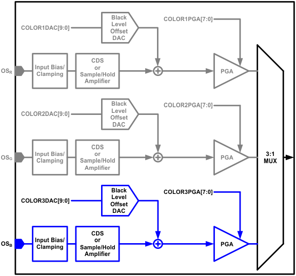 Figure 5. Mode 1a Signal Routing
Table 5. Mode 1 Operating Details
| DETAIL | |||
|---|---|---|---|
| Channels Active | OSR or OSG or OSB | One color active for all lines. | |
| Channel Sample Rate | 22.5 | MSPS per Channel (max) | |
| ADC Sample Rate | 22.5 | MSPS (max) | |
| fADC: fINCLK | Internal 1x Clock Selected | 1:1 | fINCLK = 25MHz (max) |
| Output Sequencing | SH Signal → Color 1→Color 1→Color 1→Color 1→Color 1→ | ||
Table 6. Modes of Operation Register Settings Table
| OPERATING MODE | SAMPLING INPUT(S) |
SIGNAL PATH(S) |
OUTPUT SEQUENCING MODE 3 and 2 = PIXEL SEQ |
|---|---|---|---|
| Mode3-RGB Forward | OSR||OSG||OSB | RGB | PixelR→PixelG→PixelB→ |
| Mode3-RGB Reverse | OSR||OSG||OSB | RGB | PixelB→PixelG→PixelR→ |
| Mode2-RG Forw. | OSR||OSG | RG | PixelR→PixelG→ |
| Mode2-RG Rev. | OSR||OSG | RG | PixelG→PixelR→ |
| Mode2-GB Forw. | OSG||OSB | GB | PixelG→PixelB→ |
| Mode2-GB Rev. | OSG||OSB | GB | PixelB→PixelG→ |
| Mode2-RB Forw. | OSR||OSB | RB | PixelR→PixelB→ |
| Mode2-RB Rev. | OSR||OSB | RB | PixelB→PixelR |
| Mode1-R Mono | OSR | R | Color Line Seq: R→R→R→R→ |
| Mode1-G Mono | OSG | G | Color Line Seq: G→G→G→G→ |
| Mode1-B Mono | OSB | B | Color Line Seq: B→B→B→B→ |
| CISa | Mode 1 or 2 or 3 | Any | 2, 3, or 4 lines in sequence |
| Gain and Offset are channel specific. | |||
| LM98714 style CB bits indicate channel used to process data. Additional CB bits can be used to identify current line in sequence. | |||
| CISb | Mode 1 or 2 or 3 | Any | 2 or 3 lines in sequence |
| Gain and Offset for all channels are common, and change from line to line based on current color in sequence. | |||
| LM98714 style CB bits indicate channel used to process data. Additional CB bits can be used to identify current line in sequence. |
7.4.4 Input Bias and Clamping
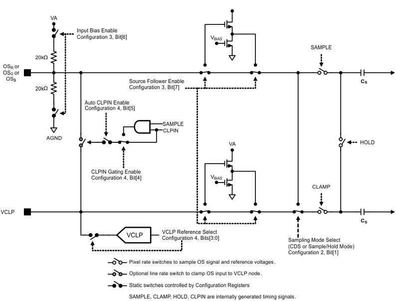 Figure 6. Input Bias and Clamping Diagram
7.4.4.1 Input Bias and Clamping - AC Coupled Applications
The inputs to the LM98722 are typically AC coupled through a film capacitor and can be sampled in either Sample and Hold Mode (S/ H Mode) or Correlated Double Sampling Mode (CDS Mode). In either mode, the DC bias point for the LM98722 side of the AC coupling capacitor is set using the circuit of Figure 6 which can be configured to operate in a variety of different modes. A typical CCD waveform is shown in Figure 7. Also shown in Figure 7 is an internal signal “SAMPLE” which can be used to “gate” the CLPIN signal so that it only occurs during the “signal” portion of the CCD pixel waveform.
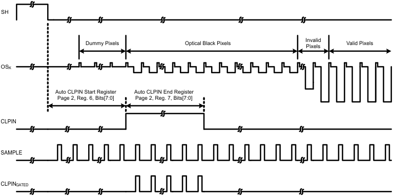 Figure 7. Typical CCD Waveform and LM98722 Input Clamp Signal (CLPIN)
7.4.5 Sample/Hold Mode
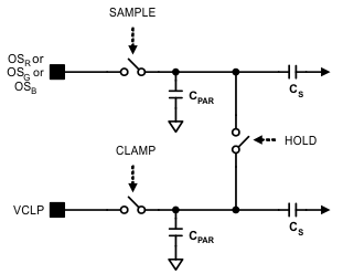 Figure 8. Sample and Hold Mode Simplified Input Diagram
Proper DC biasing of the CCD waveform in Sample and Hold mode is critical for realizing optimal operating conditions. In Sample/ Hold mode, the Signal Level of the CCD waveform is compared to the DC voltage on the VCLP pin. In order to fully utilize the range of the input circuitry, it is desirable to cause the Black Level signal voltage to be as close to the VCLP voltage as possible, resulting in a near zero scale output for Black Level pixels.
In Sample/Hold Mode, the DC bias point of the input pin is typically set by actuating the input clamp switch (see Figure 8) during optical black pixels which connects the input pins to the VCLP pin DC voltage. The signal controlling this switch is an auto-generated pulse, CLPIN. CLPIN is generated with a programmable pixel delay with respect to the SH Interval and a programmable # of pixels Duration. These parameters are available through the serial interface control registers.
Actuating the input clamp will force the average value of the CCD waveform to be centered around the VCLP DC voltage. During Optical Black Pixels, the CCD output has roughly three components. The first component of the pixel is a “Reset Noise” peak followed by the Reset (or Pedestal) Level voltage, then finally the Black Level voltage signal. Taking the average of these signal components will result in a final “clamped” DC bias point that is close to the Black Level signal voltage.
To provide a more precise DC bias point (that is, a voltage closer to the Black Level voltage), the CLPIN pulse can be “gated” by the internally generated SAMPLE clock. This resulting CLPINGATED signal is the logical “AND” of the SAMPLE and CLPIN signals as shown in Figure 7. By using the CLPINGATED signal, the higher Reset Noise peak will not be included in the clamping period and only the average of the Reset Level and Black Level components of the CCD waveform will be centered around VCLP.
7.4.6 DC Coupled Applications
In some applications, particularly with CIS sensors, the output voltage is within a voltage range that will allow DC coupling of the signal. When using Sample/Hold mode, DC coupling eliminates any problems with signal droop across the line caused by voltage changes across the coupling capacitor. When DC coupling, the Auto CLPIN should be disabled.
There are two ways of setting the proper DC levels in this type of application. If the sensor has a Vref output pin, this can be connected to the VCLP pin of the LM98722. The internal VCLP generation should be disabled to allow this external reference to set the Black Level for the chip close to the black pixel level of the sensor.
Many CIS sensors will not have a Vref output. In these applications, the internal VCLP voltage of the LM98722 can be set to the level that is closest to the black pixel level of the sensor.
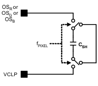 Figure 9. Equivalent Input Switched Capacitance S/H Mode
In Sample and Hold Mode, the impedance of the analog input pins is dominated by the switched capacitance of the CDS/Sample and Hold amplifier. The amplifier switched capacitance, shown as CS in Figure 8, and internal parasitic capacitances can be estimated by a single capacitor switched between the analog input and the VCLP reference pin for Sample and Hold mode. During each pixel cycle, the modeled capacitor, CSH, is charged to the OSX-VCLP voltage then discharged. The average input current at the OSX pin can be calculated knowing the input signal amplitude and the frequency of the pixel. If the application requires AC coupling of the CCD output to the LM98722 analog inputs, the Sample and Hold Mode input bias current may degrade the DC bias point of the coupling capacitor. To overcome this, Input Source Follower Buffers are available to isolate the larger Sample and Hold Mode input bias currents from the analog input pin (as discussed in Input Source Follower Buffers). As shown in CDS Mode section, the input bias current is much lower for CDS mode, eliminating the need for the source follower buffers.
7.4.7 Input Source Follower Buffers
The OSR, OSG, OSB inputs each have an optional Source Follower Buffer which can be selected with Main Configuration Register 3 at Page 0, Register 3, Bit[7]. These source followers provide a much higher impedance seen at the inputs. In some configurations, such as Sample and Hold Mode with AC coupled inputs, the DC bias point of the input nodes must remain as constant as possible over the entire length of the line to ensure a uniform comparison to reference level (VCLP in this case). The Source Followers effectively isolate the AC input coupling capacitor from the switched capacitor network internal to the LM98722’s Sample and Hold/ CDS Amplifier. This results in a greatly reduced charge loss or gain on the AC Input coupling capacitor over the length of a line, thereby preserving its DC bias point.
The Source Followers should only be used in the 1.2 V input range (i.e. Gain Mode Register at Page 1, Register 0, Bit[0] = 1, CDS Gain = 2x). Using the Source Followers in the 2.4 V (that is, Gain Mode Register at Page 1, Register 0, Bit[0] = 0, CDS Gain = 1x). Input range will result in a loss of performance (mainly linearity performance at the high and low ends of the input range).
7.4.8 CDS Mode
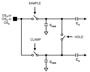 Figure 10. CDS Mode Simplified Input Diagram
Correlated Double Sampling mode does not require as precise a DC bias point as does Sample and Hold mode. This is due mainly to the nature of CDS itself, that is, the Video Signal voltage is referenced to the Reset Level voltage instead of the static DC VCLP voltage. The common mode voltage of these two points on the CCD waveform have little bearing on the resulting differential result. However, the DC bias point does need to be established to ensure the CCD waveform’s common mode voltage is within rated operating ranges.
The CDS mode biasing can be performed in the same way as described in Sample/Hold Mode, or, an alternative method is available which precludes the need for a CLPIN pulse. Internal resistor dividers can be switched in across the OSR, OSG, and/or OSB inputs to provide the DC bias voltage.
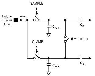 Figure 11. CDS Mode Input Bias Current
Unlike in Sample and Hold Mode, the input bias current in CDS Mode is relatively small. Due to the architecture of CDS switching, the average charge loss or gain on the input node is ideally zero over the duration of a pixel. This results in a much lower input bias current, whose main source is parasitic impedances and leakage currents.
As a result of the lower input bias current in CDS Mode, maintaining the DC Bias point the input node over the length of a line will require a much smaller AC input coupling capacitor.
7.4.9 VCLP DAC
The VCLP pin provides the reference level for incoming signals in Sample and Hold Mode. The pin’s voltage can be set by writing to the VCLP Configuration Register on register page 0. By default, the VCLP pin voltage is established by an internal resistor divider which sets the voltage to 0.85 VA.
The VCLP buffer can also be disconnected and the pin driven externally by the another voltage in the application, such as Vref from some CIS sensors.
Table 7. VCLP Voltage Setting
| VCLP CONFIGURATION PAGE 0, REGISTER 0x04, BITS[2:0] |
TYPICAL VCLP OUTPUT (FINAL SILICON TARGETS) |
|---|---|
| 000 | 0.85VA (Default) |
| 001 | 0.9VA |
| 010 | 0.95VA |
| 011 | 0.6VA |
| 100 | 0.55VA |
| 101 | 0.4VA |
| 110 | 0.35VA |
| 111 | 0.15VA |
7.4.10 Gain and Offset Correction
Each input channel has individual settings for offset (DAC) and gain (PGA and CDS/SH gain).
7.4.10.1 Analog Offset
Analog offset (DAC) settings are individually adjustable for each color. In addition, there are (optionally) separate settings for Even and Odd pixels being processed through each color channel. This feature is designed to support specific CCD sensors that have two CCD transfer arrays per color, which may introduce different offset for the Even versus Odd pixels.
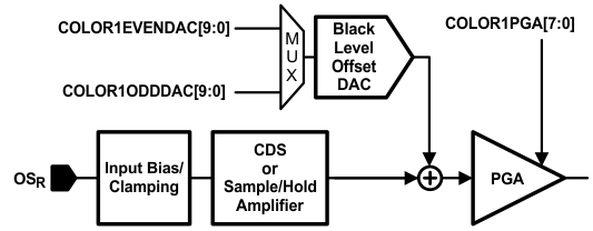 Figure 12. Analog Offset Applied Prior to PGA
The Black Level Offset DACs are set with a 9 bit plus sign value. This gives an approximate adjustment range of +/- 300 mV or +/- 600mV when the CDS/SH Gain is set to 1x or 2x.
The analog offset registers are found at Page 1, Registers 0x04h to 0x0Fh.
7.4.10.2 Digital Offset
In addition, digital offset can be added to color data at the output of the ADC in the Digital Offset block. The digital offsets are a +/- 6 bit value. This value is summed with the upper 11 bits of the ADC output. Therefore, the effective offset range is from +2016 to -2048 lsbs of the ADC output.
The digital offset registers are found at Page 1, Registers 0x10h to 0x15h.
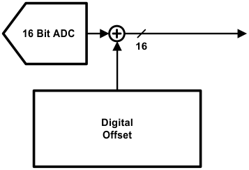 Figure 13. Digital Offset Applied to ADC Output
7.4.10.3 Even/Odd Offset Coefficients
Certain CCD sensors may have different offset voltages for the Even versus the Odd pixels. To optimize the image processing of these pixels, separate coefficients can be stored, and applied for the Even and Odd pixels. The Even/Odd offset feature is enabled by setting Page 0, Register 0x02h, Bit 0 = 1. Bimodal correction, discussed below, is automatically disabled when Even/Odd offset coefficients are enabled.
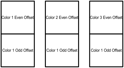 Figure 14.
-
Analog Gain
- The gain of each input channel can be adjusted at two points in the signal chain.
-
CDS/SH Gain - Page 1, Register 0x00h
- A 1x or 2x gain setting is available in the CDS/SH amplifier.
- By default, one common CDS/SH gain setting setting is used for all input channels. If desired, individual CDS/SH gain settings can be used for each input. To enable this feature, set Page 1, Register 0x00h, Bit 2 = 1.
-
PGA Gain - Page 1, Registers 0x01h, 0x02h, 0x03h
- An 8 bit PGA (Programmable Gain Amplifier) is also available. The PGA gain curve is non-linear for optimal performance in imaging applications, and is shown on Figure 15. The approximate gain equation is:
Equation 1. Gain (V/V) = 180/(277-PGA_Code), Gain (dB) = 20log10(180/(277-PGA_Code))
The gain setting registers are found at Page 1, Registers 0x00h, 0x01h, 0x02h and 0x03h.
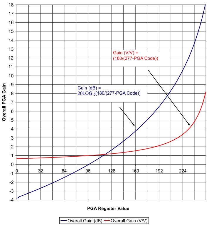 Figure 15. PGA Gain vs. PGA Gain Code
-
Dual Gain Mode - Page 1, Register 0x00h, Bit 1, and Registers 0x16h, 0x17h, 0x18h
- In many scanning systems, the system illumination and optics characteristics will result in a much higher optical efficiency in the pixels near the middle of the sensor, compared with the pixels at the beginning and end of the sensor. If a single gain setting is used for all pixels, the middle pixels will be near clipping, while the ones at the edges can be at 1/2 scale or lower. This results in lower signal to noise for the edge pixels. To combat this problem, the LM98722 incorporates an optional Dual Gain system. When enabled, the system provides a second set of PGA gain registers to set the “high” gain for each input channel. The “normal” gain settings will be applied during the “active/white” pixels, while the “high” gain settings will be applied for all pixels before and after the “active/white” pixels (see Figure 16).
- The Dual Gain enable bit is found at Page 1, Register 0x00h, Bit 1. The High Gain PGA settings are found at Page 1, Registers 0x16h to 0x18h.
7.4.11 LM98722 Typical Line Timing and Pixel Gain Regions
7.4.12 Automatic Black and White Level Calibration Loops
7.4.12.1 Calibration Overview
The offset and gain settings in the AFE will normally be set to optimize the range of the sensor output signal within the ADC input range. These settings can be calculated in a host ASIC and loaded into the AFE during the calibration procedure. To reduce the processing required to do these calculations, the LM98722 has built in feedback or calibration loops that will automatically adjust the offset and gain settings. A number of register values must be initially set to optimize the calibration for the particular application.
7.4.12.2 Different Modes for Different Needs
The calibration features of the LM98722 are not intended to be used during active scanning, but rather before scanning begins, or in the page gap between images. Generally, more time is available to perform the initial calibration before scanning begins. Page gap calibration must be necessariliy short to ensure the process finishes in the limited number of scan lines available.
The Black and White Fine Tuning, and Black Calibration Only modes can be used during the page gap to adjust for small differences in offset/gain that occur over time.
Black and White Full Calibration should be run before the initial scanning process, or periodically between major jobs to take care of larger shifts in offset/gain of the input signal.
7.4.12.3 Calibration Initiation
Once these settings have been made, the Register Lock Control bit (Page 0, Register 0, Bit 0) should be set to begin converting pixels. Once the sensor data from the test image is stable the calibration process can be started by either setting the CAL register bit at Page 0, Register 0x01h, Bit 5, or by applying a logic high to the CAL input pin. (Both of these inputs are active when the Register Lock Control is set.) The CAL input pin is particularly useful for implementing page gap calibration.
7.4.12.4 Key Calibration Settings
Table 8. Key Calibration Settings
| General Settings | ||
| Calibration Mode | Page 2, Register 0, Bits[1:0] | |
| Black Calibration Only | 00 | |
| Black and White Full Calibration | 01 | |
| Black and White Fine Tuning: | 10 | |
| Number of Lines | Page 2, Register 1 | |
| Black Loop Specific Settings | ||
| # Black Pixels Averaged | Page 2, Register 2, Bits[1:0] | |
| Black Target | Page 2, Register 3 | |
| Black Pixels Start | Page 2, Register 8 | |
| ADAC Scaling | Page 2, Register 2, Bits[3:2] | |
| DDAC Scaling | Page 2, Register 2, Bits[5:4] | |
| DDAC enable/disable | Page 2, Register 0, Bit 2 | |
| White Loop Specific Settings | ||
| White Target | Page 2, Register 5 | |
| White Loop Tolerance | Page 2, Register 4, Bits[6:3] | |
| White Pixel Averaging Window Size | Page 2, Register 4, Bits[2:0] | |
| Active/White Pixels Start | Page 2, Registers 0x09h, 0x0Ah | |
| Active/White Pixels End | Page 2, Registers 0x0Bh, 0x0Ch | |
The calibration loops are intended to be used prior to scanning the page or between pages being scanned. The black loop calibrates the channel offset such that the ADC outputs the desired code for Optical Black Pixels. The white loop calibrates the channel gain such that the ADC outputs the desired maximum white value when scanning a white target image.
The Black Loop and White loop will both update until the # Lines setting is met. Settings of 1 to 254 lines will cause the loops to run for that many lines, and then stop. A setting of 255 will cause the calibration loops to run indefinitely.
While using the Auto Black Level Correction Loop, the DAC registers are re-written as required every line the loop is running.
While using the Auto White Level Correction Loop, the PGA registers are re-written as required every line the loop is running.
7.4.12.5 General Black Loop Operation
During calibration, the following general process is performed:
Beginning at Black Pixels Start, the selected number of black pixels are averaged.
This Black Average value is compared with the Black Target to give the Black Error value.
In general, if the Black Average>> Black Target, the new DAC values will be lower than the previous ones. If the Black Average < Black
Target the new DAC values will be higher than the previous ones.
The ADAC Scaling and DDAC Scaling values are used to balance the speed of convergence against the tolerance for noise in the data. The smallest (1/8) scaling values will give slower convergence, but will make the system respond more slowly to noisy data. The highest (1/2) will result in the fastest convergence, but will respond more quickly to noisy data. The DDAC scaling factor of Linear - 1LSB adjust will result in a maximum change of one LSB of the DDAC value, regardless of how great the difference between Black Average and Black Target
The number of Black Pixels to be processed by the algorithm is set at Page 2, Register 2, Bits[1:0]. 4, 8, 16 or 32 pixels can be averaged together to determine the current Black Value. Averaging the highest number of pixels possible for the sensor in use will improve the accuracy and repeatability of the Black Average value.
The delay from the end of the SH Interval to the first Black Pixel to be processed is set at Page 2, Register 8. A delay of up to 255 pixels can be set.
7.4.12.6 ADAC/DDAC Convergence
At the beginning of the calibration process, the ADAC will be used to reduce the Black Error as much as possible. Once further adjustments of the ADAC can no longer reduce the Black Error, the ADAC adjustments will stop and the DDAC will be used. *If users would rather apply digital offset corrections in their ASIC, the DDAC corrections can be omitted by setting the DDAC disable bit at Page 2, Register 0x00h, Bit 2.
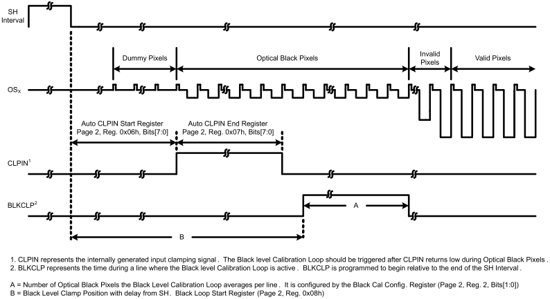 Figure 17. Black Loop Timing
7.4.12.7 General White Loop Operation
The White Peak value is determined by a moving window average done throughout the Active/White pixels region of the line (see to Figure 16). The size of the moving window is set at Page 2, Register 4, Bits[2:0]. 4, 8, 16 or 32 (default) pixels are averaged together at a time and compared with the previous Peak White value. If the new White Average is greater than the previous Peak White value, then the Peak White value is set equal to the White Average. The window is then shifted over to the next group of pixels (one window width) and a new average is calculated. This process is repeated until the Active/White Pixels End value is reached. The final Peak White value is then compared with the White Target value (Page 2, Register 5). The gain settings are then adjusted to make the Peak White value closer to the White Target value.
7.4.12.8 White Loop Modes
- White Full Calibration (Cold start or Pre-Job): In this mode, the gain settings are completely reset to default at the beginning of the loop. The first change or gain decision is whether the CDS/SH gain setting will be 1x or 2x. Subsequent decisions are made to adjust the PGA setting to the provide the Peak White value that is closest to the White Target value
- White Fine Tuning (Page Gap Calibration): In this mode, the previous gain settings are used as the starting point. The CDS/ SH gain setting will not be changed. The PGA gain will be increased or decreased by one step at a time, to fine tune the gain. This mode is normally used where only minor changes in the white level are expected.
7.4.12.9 Bimodal (Automatic) Correction
Due to the architecture of the ADC used in the LM98722, it is possible that a small offset in the resulting data will be present between the Even and Odd pixels processed by the device. This offset is referred to as a Bimodal distribution in the data. It can occur because the signals being processed go through two different paths to achieve the required throughput. Each of these paths can give a slightly different signal offset, resulting in the bimodal distribution in output data, for a given fixed input voltage.
When the automatic Black Level (offset) correction circuit is engaged, a portion of that circuitry automatically corrects the bimodal distribution. The bimodal correction applied is stored at Page 1, Registers 0x1Ch, 0x1Dh, and 0x1Eh. The stored value is divided by two. Half is added to the Even pixels, and half is subtracted from the Odd pixels.
7.4.13 Coarse Pixel Phase Alignment
Precise placement of the CCD video signal sampling point is a critical aspect in any typical imaging application. Many factors such as logic gate propagation delays and signal skew increase the difficulty in properly aligning the CCD pixel output signals with the AFE input sampling points. The LM98722 provides two powerful features to aid the system level designer in properly sampling the CCD video signal under a large range of conditions. The first feature, discussed in this section, is the Coarse Pixel Phase Alignment block. As the name implies, this block provides a very coarse range of timing adjustment to align the phase of the CCD Pixel output with the phase of the LM98722 sample circuit. The second feature, discussed in Internal Sample Timing, is the block which is designed for fine tuning of the sampling points within the selected Coarse Pixel Alignment Phase. A small portion of a typical imaging application is shown in Figure 18.
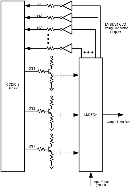 Figure 18. Typical AFE/CCD Interface
As shown in Figure 18, the LM98722 provides the timing signals to drive the CCD using external logic gates to drive the high capacitance CCD clock pins. The pixels are shifted out of the CCD, thru the emitter follower buffers and received by the LM98722 inputs for processing.
In an ideal application, depicted in Figure 19, the Pixel output signal would be in phase with the timing signals that drove the CCD. The LM98722 input sampling clocks (CLAMP and SAMPLE) are adjustable within a pixel period. By default, the pixel period (or pixel “phase”) is defined to be in line with the input clock. As shown in the ideal case, Figure 19, CLAMP and SAMPLE can be properly adjusted to their ideal positions within the pixel phase, shown in Figure 19 at the stable region near the end of the pedestal and data phases.
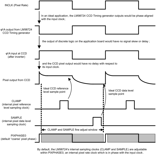 Figure 19. Clock Alignment in an Ideal Application
However, in a real system, propagation delays exist in all stages of the signal chain. These propagation delays will lead to a shift in the CCD Pixel outputs with respect to the LM98722 input clock. The phase shift of the CCD Pixel output, demonstrated in Figure 20, can lead to significant sample timing issues if not properly corrected.
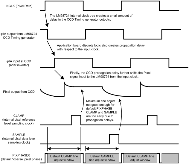 Figure 20. CCD Output Phase Shift in a Real Application
In the default mode, the LM98722 sampling is performed during a clock period whose phase is aligned with the input clock (ignoring any clock tree skew for the moment). The actual sampling clocks are adjustable within the clock period, as shown in Figure 21 (shown for CDS mode in Figure 20) and further described in Internal Sample Timing . As shown in Figure 20, the delay of the CCD Pixel output is shifted far enough that the fine CLAMP and SAMPLE clocks cannot be placed in a stable portion of the waveform. To remedy this situation, the LM98722’s Coarse Pixel Phase Alignment feature allows the designer to shift the entire phase of the analog front end with respect to the input clock. This allows the designer to choose one of four sampling phases which best matches the delay in the external circuitry. Once the “Coarse Pixel Phase” has been chosen, the designer can then fine tune the sampling clocks using the fine adjustment (see Internal Sample Timing).
The four available Coarse Pixel Phases (PIXPHASE0 - PIXPHASE3) are depicted in Figure 21 (Mode 3), Figure 22 (Mode 2) and Figure 23 (Mode 1). Also shown in the diagrams are the external input clock (INCLK) and a typical CCD output delayed from the input clock.
7.4.14 Internal Sample Timing
A typical CCD input signal is depicted in Figure 24 and Figure 25. Also shown are the internally generated SAMPLE and CLAMP pulses. These signals provide the sampling points of the input signal (OSX). The timing of SAMPLE and CLAMP is derived from an internal system clock (SYSCLK).
The pixel’s reference level input (depicted as VREF) is captured by the falling edge of the CLAMP pulse. In Sample/Hold Mode the VREF input is a sample of the VCLP DC voltage. In CDS Mode the CLAMP pulse samples the pedestal Level of the CCD output waveform.
The pixel’s signal level input (depicted as VSIG) is captured by the SAMPLE pulse. In either Sample/Hold or CDS Mode, the VSIG input is the signal level of the CCD output waveform.
The LM98722 provides fine adjustment of the CLAMP and SAMPLE pulse placement within the pixel period. This allows the user to program the optimum location of the CLAMP and SAMPLE falling edges. The available fine tuning locations for CLAMP and SAMPLE are shown in Figure 25 and Figure 27 for each sampling mode (CDS or S/H) and channel mode (3, 2, or 1 Channel).
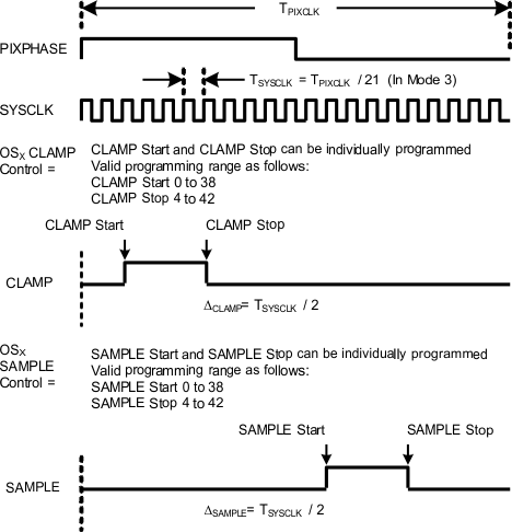 Figure 26. 3 Channel (Mode 3) CLAMP and SAMPLE Timing
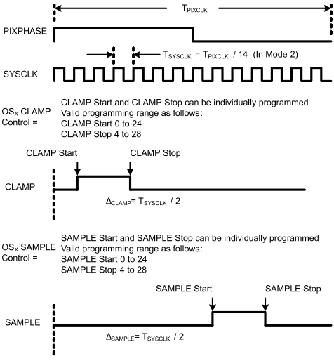 Figure 27. 1 or 2 Channel (Mode 1, Mode 2) CLAMP and SAMPLE Timing
7.4.14.1 CCD Timing Generation
A flexible internal timing generator is included to provide clocking signals to CCD and CIS sensors. A block diagram of the CCD Timing Generator is shown in Figure 28.
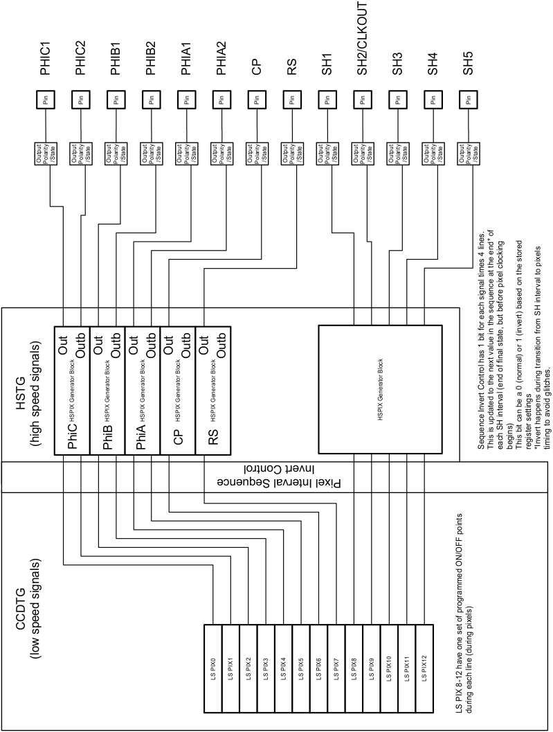 Figure 28. CCD Timing Generator Block Diagram
Examples of the various operating modes and settings are shown in Figure 29 through Figure 32. The detailed pixel timing is somewhat dependent on the operating modes of the AFE circuitry regarding the number of adjustment points for the on and off points of the different timing outputs.
Note: In addition to the timing adjustments shown, the polarity of all sensor clock signals can be adjusted by register control.
7.4.14.2 SH Interval Details - Multiple States Defined within SH Interval
In the LM98722, each SH Interval (the period when the high speed pixel timing is stopped) can have a selected number of “States”, with each “State” having a specified duration. In the most common usage, each SH Interval is the same, and there can be as many as 31 defined States within the SH Interval. During each State, the logic level of each output signal can be defined as 1 or 0. The duration of the State, and the logic levels of the signals are defined in configuration registers on register pages 3, 4 and 5.
Each State basic duration can be from 1 to 255 pixel periods. There is also a multiplier of 2x, 4x, 8x or 16x (Page 2, Register 0x17) that will increase SH State durations for sensors that require long SH pulse widths
If less than the maximum number of states are required, the first 0 duration State in the SH Interval will terminate processing.
At the end of the SH Interval, a glitchless transition to pixel timing will occur. Similarly, at the end of the pixel timing, a glitchless transition to the first state in the SH Interval will occur.
Some more complex sensors require different SH Interval timing in some sequence. The LM98722 can support up to 4 different SH Interval Timings. The available 31 states are divided as follows when higher numbers of SH Intervals are used:
Table 9. States within SH Interval Details
| AVAILABLE STATES | ||||
|---|---|---|---|---|
| # of SH Intervals | SH Interval 1 | SH Interval 2 | SH Interval 3 | SH Interval 4 |
| 1 | 0 to 30 | n/a | n/a | n/a |
| 2 | 0 to 14 | 15 to 30 | n/a | n/a |
| 3 | 0 to 9 | 10 to 19 | 20 to 30 | n/a |
| 4 | 0 to 6 | 7 to 14 | 15 to 22 | 23 to 30 |
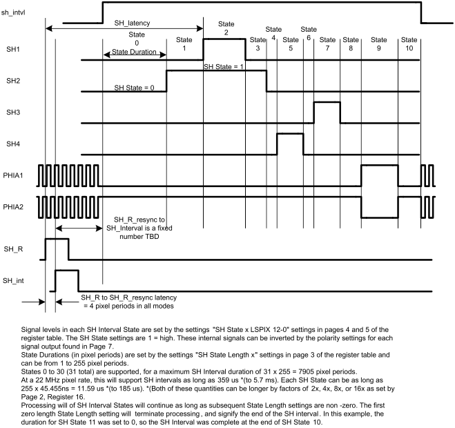 Figure 33. Sensor Timing SH Interval Details - Single SH Interval
An example showing a 4 SH Interval sequence is shown on Figure 34 through Figure 37.
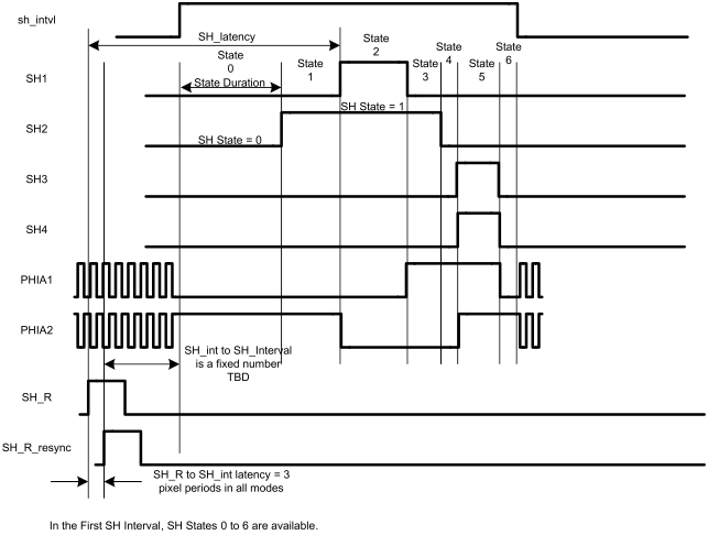 Figure 34. Sensor Timing SH Interval Details - Multiple SH Intervals - 1 of 4
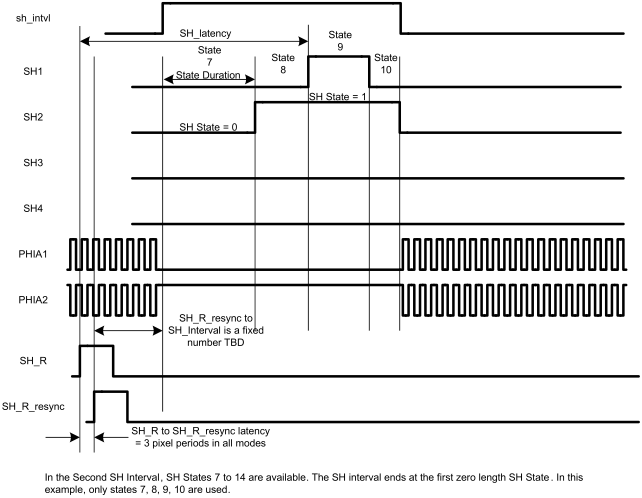 Figure 35. Sensor Timing SH Interval Details - Multiple SH Intervals - 2 of 4
 Figure 36. Sensor Timing SH Interval Details - Multiple SH Intervals - 3 of 4
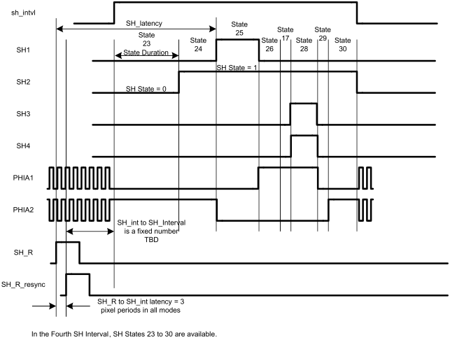 Figure 37. Sensor Timing SH Interval Details - Multiple SH Intervals - 4 of 4
7.4.14.3 SH Outputs - Low Speed Line Timing Usage
While the PHI, RS and CP outputs generate high speed timing during the pixel portion of the line, the SH outputs can be used to generate low frequency signals during this period. This can be useful to generate “mode” or “resolution” control signals for certain sensors.
Each SH output has a programmed ON and OFF point within the line. These points are programmed with a 16 bit value that sets the pixel number where the transition occurs.
Programming ON and OFF in different orders will allow pulses that are normally low or normally high, always high, always low, etc. A common 1x, 2x, or 4x multiplier (Page 2, Register 0x15) can be used to increase the range (and reduce the resolution) of these ON/ OFF points, as well as the White/Active and Line Length pixels settings.
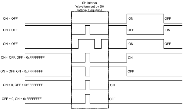 Figure 38. Sensor Timing SH ON/OFF Details - Example Settings and Waveforms
7.4.14.4 Controlled Inversion
When using multiple SH Intervals, it is possible to invert the pixel portion of the line for any of the output signals in any of the 4 Lines in the sequence. There is one bit per signal (or pair of signals for PHIA, PHIB and PHIC), for each of the 1 to 4 lines in the sequence. Setting the bit for a particular output and line in the sequence will cause the pixel portion of that line to be inverted. The transition to the next line in the sequence occurs at the end of the SH Interval. Inversion can affect both the high speed timing signals (PHIx, RS, CP) and the low speed ON/OFF behavior of the SH signals.
Figure 39 is an example of Polarity Override with a 2 Line sequence. Note that the PHIA1, SH1, SH2 and SH3 signals are inverted in Line 2, while all other signals are at the default polarity for both lines.
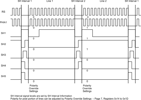 Figure 39. Sensor Timing Mode Pin Output Details - Active Programmed Transition
7.4.15 CCD Timing Generator Master/Slave Modes
The internal Sensor Timing generator is capable of operating in Master Mode or in Slave Mode. The Master/Slave operation is configured with the Master Mode Select bit (Page 0, Register 0x00, bit 1). In either Master or Slave Mode, control bit data can be included in the LM98722 output data to indicate when each new scan is starting as well as pixel information such as color, type (active, black, dummy, etc.), and the beginning of each line.
7.4.15.1 Master Timing Generator Mode
In Master Timing Mode (Page 0, Register 0x00, bit 1 = 1), the LM98722 controls the entire CCD Timing Generation based on INCLK and the Register Lock Bit (Page 0, Register 0, Bit 0) state. The Register Lock bit is set by the user to initiate a new scan. The LM98722 controls when each new line of the scan begins and ends based on the CCD Timing Generator register settings. Scanning is enabled as long as the Register Lock bit = 1. The period of the line (integration time) is controlled by the SH Interval State Length settings (Page 3 Registers) and the Line Length setting (Page 3, Registers 0x0D and 0x0E) as well as the Pixel Multiplier Factor (Page 2, Register 0x0F) and SH State Length Multiplier (Page 2, Register 0x11) .
The line period from end of one SH Interval to the end of the next SH Interval is equal to:
7.4.15.2 Slave Timing Generator Mode
In Slave Timing Mode (Page 2, Register 0x00, bit 1 = 0), the LM98722 CCD Timing Generator is controlled by the external SH_R pin. Each new line of a scan is initiated by an SH_R pulse. The period of the line (integration time) is mainly controlled by the period of the incoming SH_R signal. The minimum period between SH_R pulses should be at least the SH Interval duration as calculated in Equation 2, plus the number of pixels to be clocked out of the CCD or CIS sensor.
 Figure 40. SH_R to INCLK (PIXCLK or ADCCLK) Timing
7.4.15.3 Multiple SH Intervals
Multiple SH Intervals are supported for those CCD sensors that has different waveform and timing requirements during successive SH Intervals. Up to 4 different SH Intervals are supported.
In the Multiple SH Interval mode, the Line Period can be different for each line, due to the possible different settings for SH Interval duration. In that case the Line Periods would be calculated as follows:
Line Period1 = (Sum of SH Interval States1 x SH State Length Multiplier) + (Line Length Setting x Pixel Multiplier Factor) pixels
Line Period2 = (Sum of SH Interval States2 x SH State Length Multiplier) + (Line Length Setting x Pixel Multiplier Factor) pixels
Line Period3 = (Sum of SH Interval States3 x SH State Length Multiplier) + (Line Length Setting x Pixel Multiplier Factor) pixels
Line Period4 = (Sum of SH Interval States4 x SH State Length Multiplier) + (Line Length Setting x Pixel Multiplier Factor) pixels
In multiple SH Interval mode, the SH Interval States are subdivided as follows:
Table 10. Multiple SH Intervals Table
| # SH INTERVALS | SH INTERVAL 1 STATES | SH INTERVAL 2 STATES | SH INTERVAL 3 STATES | SH INTERVAL 4 STATES |
|---|---|---|---|---|
| 1 | 0 to 30 | |||
| 2 | 0 to 14 | 15 to 30 | ||
| 3 | 0 to 9 | 10 to 19 | 20 to 30 | |
| 4 | 0 to 6 | 7 to 14 | 15 to 22 | 23 to 30 |
7.4.15.4 Support for CIS Sensors
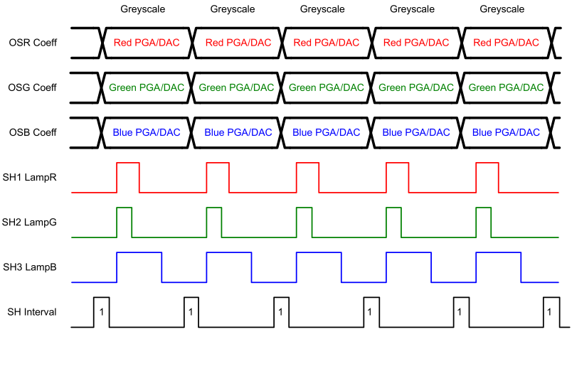
In CIS Sensor modes, the SH (LampR), SH2 (LampG), SH3 (LampB) and SH4 (LampIR) outputs are configured as Lamp illumination control outputs. In CIS mode, the number of lines/colors in the lamp sequence is selected by the Multiple SH Interval setting at Page 2, Register 10h, Bits 1:0. Sequences of 2, 3 or 4 lines/colors are supported in CIS mode. By definition, the standard CCD timing mode is equivalent to a CIS mode with length = 1.
Two different CIS modes are supported (CISa and CISb, selected at Page 2, Register 0x10h, Bits 4:3):
In CISa, there can be 2, 3 or 4 colors in the sequence, to support sensors with as many as 4 different lamp colors. In this mode, the PGA and DAC settings are controlled by the channel settings, regardless of what line in the sequence is being processed.
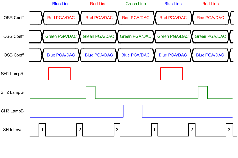 Figure 41. Mode 3, 3 Color Sequence, CISa Default
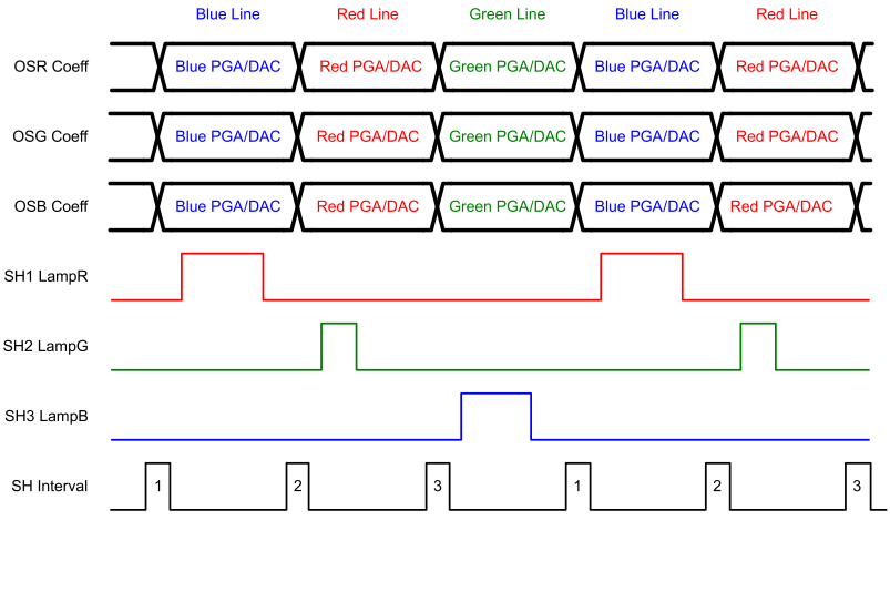 Figure 42. Mode 3, 3 Color Sequence, CISb
In CISb, when a 2 line sequence is selected, it is necessary to choose which coefficients are used during the 2 different lines in the sequence. this selection is made with the CISb Color Coefficient Select at Page 2, Register 10h, Bits 6:5. Following is an example of a 2 color sequence, where Red and Green are the selected colors:
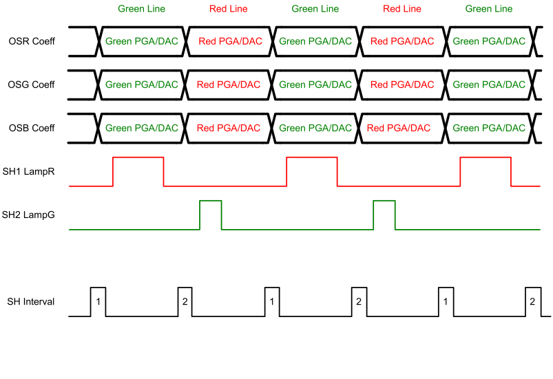
To support monochrome scanning with an RGB CIS, select Mode 3, and a 1 line sequence. The LampR, LampG and LampB On/Off times will apply for every line. The On/Off times and relative channel gains can both be adjusted to achieve the desired white balance. Lamps can be on either simultaneously if the CIS and power budget allow, or sequentially.
7.4.15.5 LVDS Output Format - LM98714 Mode
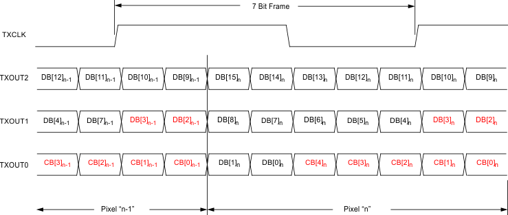 Figure 45. LVDS Output Bit Alignment and Data Format
7.4.16 LVDS Control Bit Coding - LM98714 Mode
The 5 control bits included in the LVDS data stream are coded as follows:
The "active" and "black" pixel tags are programmable tags that the LM98722 provides in order to identify how many pixels have been processed since the falling edge of SH.
Which pixels are given "Active" and "Black" CB tags is controlled by Page 2, Registers 0x02, 0x08-0x0C, and 0x0F. (# Black Pixels Averaged, Black Pixels Start, Active/White Pixels Start, Active/White Pixels End, and Line Length Multiplier).
The LM98722 counts the number of pixel periods after the SH Interval: If the number of pixel periods after the SH Interval is greater than (Black Pixels Start) and less than (Black Pixels Start + # Black Pixels Averaged) the CB bits will indicate that the pixel is a Black pixel. If the number of pixel periods after the falling edge of SH is between Active/White Pixels Start and Active/White Pixels End, the CB bits will indicate that the pixel is an Active pixel.
7.4.16.1 Latency Compensation of CB Bits
By default, the CB bits will be compensated for the latency through the AFE signal chain. This compensation can be turned off by setting Page 8, Register 0x08, Bit 2 = 1.
Table 11. Latency Compensation of CB Bits
| BITS | DESCRIPTION |
|---|---|
| CB[4] | |
| 0 | Not the beginning of line |
| 1 | Beginning of Line (This bit is high during the SH Interval) |
| CB[3:0] | |
| 0000 | Dummy Pixels |
| 0001 | Red Active Pixels |
| 0010 | Green Active Pixels |
| 0011 | Blue Active Pixels |
| 0100 | IR1 Active Pixels |
| 0101 | IR2 Active Pixels |
| 0110 | Red Black Pixels |
| 0111 | Green Black Pixels |
| 1000 | Blue Black Pixels |
| 1001 | IR1 Black Pixels |
| 1010 | IR2 Black Pixels |
| 1111 | Beginning of Scan (This bit is high during the SH Interval of the first line after the Lock Bit transitions from low to high) |
7.4.17 Flexible LVDS Formatting Mode: Mapping
 Figure 46. LVDS Output Bit Alignment and Data Format
In Flexible LVDS Formatting Mode, the values highlighted in red can be substituted with other CB tag information. Table 12 shows the different CB information that can be selected:
Table 12. Selectable CB Tag Information
| SETTING | CB TAG INFORMATION |
|---|---|
| 0000 | Original CB or Data |
| 0001 | CBO0 from LM98714 definition |
| 0010 | CBO1 from LM98714 definition |
| 0011 | CBO2 from LM98714 definition |
| 0100 | CBO3 from LM98714 definition |
| 0101 | CBO4 from LM98714 definition |
| 0110 | R - High for a red channel pixel |
| 0111 | G - High for a green channel pixel |
| 1000 | B - High for a blue channel pixel |
| 1001 | Parity - 21 bit if TXOUT0 Enabled, 14 bit if TXOUT0 Disabled |
| 1010 | Ping - High for pixels processed by the Ping section of a channel, low for Pong |
| 1011 | Line# lsb - Line = 0 to 3 for lines 0 to 3 in multiline sequences |
| 1100 | Line# msb |
| 1101 | Black Loop Pixels - High for pixels processed by the Black Loop |
| 1110 | White Loop Pixels - High for pixels process by the White Loop |
| 1111 | CLP Pixels - High for pixels where the input CLP switch is closed |
7.4.17.1 TXOUT0 Disable
The TXOUT0 data pair can be disabled. In combination with the new Flexible LVDS Formatting Mode, this can support applications where only the upper 14 MSB of data are required. This will save one pair of LVDS wires in the cable, and reduce the LM98722 slightly.
In addition, if fewer than 14 bits are required, the D2 and D3 bits can be replaced with the desired CB information, selected from Table 12.
7.4.17.2 Parity
A parity bit is available for use as one of the CB bits. Parity is calculated based on all bits being sent via the 21 or 14 bit LVDS link except:
- If any bit is selected to transmit CB Parity, it will not be used in the calculation
- If any bit is transmitting a scrambler key bit when scrambler mode 2 is selected, it will not be used in the calculation.
The total parity across the 21 or 14 output bits (excluding any scrambler key bit) will be even.
7.4.17.3 Latency Compensation of CB Bits
By default, the CB bits will be compensated for the latency through the AFE signal chain. This compensation can be turned off by setting Page 8, Register 0x08, Bit 2 = 1.
7.4.18 LVDS Data Randomization for EMI Reduction
While LVDS transmissions will inherently reduce the amount of electromagnetic energy, further reductions can be achieved by randomizing the data being sent over the link. A built in “scrambler” feature provides a number of different modes to suit different applications and host processing capabilities. One key part of the scrambler is a linear feedback shift register (LFSR) implementation to provide pseudo-random sequence “keys” to randomize the image data. The basic implementation of an LFSR is shown in Figure 47:
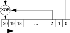 Figure 47. Basic Implementation of an LFSR
The LFSR algorithm used in the LM98722 is an n=21 maximal length right-shift implementation as shown in Figure 47. As a reference for FPGA and ASIC developers, the sequence is the same as that created by the Synopsys DW component DW03_lfsr_load with inverted outputs. The preload or starting value for the sequence is 0x000001h.
If the prs (serial-type) output is selected (MODE = 01, SUB_MODE = 0X), the 21 bits of the LFSR are shifted one position to the right on each TXCLK.
For clarity, the first 11 values in the prs sequence are:
0x000001h
0x100000h
0x080000h
0x040000h
0x020000h
0x010000h
0x008000h
0x004000h
0x002000h
0x001000h
0x000800h
If the pprs (parallel-type) output is selected (MODE = 01, SUB_MODE = 1X), the next 21 coefficients of the shift-in term are calculated in parallel, and the LFSR is loaded with these coefficients: the effect is equivalent to clocking the LFSR 21 times in serial mode. For clarity, the first 11 values in the pprs sequence are:
0x000001h
0x080001h
0x020001h
0x0A8001h
0x002001h
0x082801h
0x022201h
0x0AAA81h
0x000021h
0x080029h
0x120023h
A summary and description of each of the modes and submodes is shown in Table 13.
Table 13. Mode and Submode Summary
| MODE Page 0, Register 0x05 Bits 4:3 |
SUB_MODE Page 0, Register 0x05 Bits 2:1 |
DESCRIPTION |
|---|---|---|
| 00 | Scrambler Disabled | |
| 01 | Full Scrambler Enabled. Sub-mode Settings Select: | |
| 00 | send lvds_data[20:0] bitwise XOR with prs[20:0] | |
| 01 | send prs[20:0] | |
| 10 | send lvds_data[20:0] bitwise XOR with pprs[20:0] | |
| 11 | send pprs[20:0] | |
| 10 | 1 bit scrambler with key of prs[0] send lvds_data[20:0] bitwise XOR with prs[0], with lvds_data[k] = 0 send prs[0] on lvds_out[k] k is selected with following settings: | |
| 00 | k = 0 (DB0 in CMOS and 714 modes, CB0 in flexible, 16 bit mode) | |
| 01 (TXOUT0 Disable = 0) | k = 5 (DB0 (LSB) in flexible, 16 bit mode) | |
| 01 (TXOUT0 Disable = 1) | k = 7 (DB2 (LSB) in flexible, 14 bit mode) | |
| 10 | k = 16 (CB0 in 714 mode) | |
| 11 | k = 20 (CB4 in 714 mode) | |
| 11 | 1 bit scrambler with key of lvds_data[k]. send lvds_data[20:0] bitwise XOR with lvds_data[k] with lvds_out[k] = lvds_data[k]: | |
| 00 | k = 0 (DB0 in CMOS and 714 modes, CB0 in flexible, 16 bit mode) | |
| 01 (TXOUT0 Disable = 0) | k = 5 (DB0 (LSB) in flexible, 16 bit mode) | |
| 01 (TXOUT0 Disable = 1) | k = 7 (DB2 (LSB) in flexible, 14 bit mode) | |
| 10 | k = 16 (CB0 in 714 mode) | |
| 11 | k = 20 (CB4 in 714 mode) | |
7.4.18.1 Mode 00: Scrambler Disabled
Mode 00: Scrambler Disabled
7.4.18.2 Mode 01: Full Scrambler Using The Full 21-bit Pseudo Random Sequence
There are 4 sub-modes: (a) the 21-bit output will be bit-wise XORed with the 21-bit serial pseudo-random sequence. i.e. lvds_data[20:0] ^ prs[20:0]; (b) the 21-bit serial pseudo random sequence will be output directly; (c) the 21-bit output will be bit-wise XORed with the 21-bit parallel pseudo-random sequence. i.e. lvds_data[20:0] ^ pprs[20:0]; (d) the 21-bit parallel pseudo random sequence will be output directly. In all sub-modes, the sequences start m clock cycles after the de-assertion of the bol where m is defined as the analog latencies in 1-ch, 2-ch and 3-ch modes. In other words, the output starts the same way as the up-count test pattern mode. Unlike the up-count test pattern mode, the 21-bit pseudo-random sequence runs at the ADC (same as TXCLK) rate, not pixel or line rate.
7.4.18.3 Mode 10: One bit scrambler using the prs shift bit only, sending this bit out on a CB bit
Each bit of lvds_data[20:0] is XORed with prs[0]. One selected bit, lvds_data[k] is replaced with 0 before the XOR procedure. The resulting output lvds_out[20:0] has bit k replaced by prs[0]. The bit k selection is flexible to support different mappings of lvds_out depending on output settings as follows:
- LVDS Mapping - 714 Default Mode versus Flexible Mode (Since the location of CB bits changes depending on which is selected) Mapping select is at Page 8, Register 8, Bit 0.
- CMOS Mode versus LVDS Mode (since only lvds_out[15:0] are available in CMOS mode) CMOS/LVDS mode select at Page 0, Register 5, Bit 7.
- LVDS 3 Pair Mode versus LVDS 2 Pair Mode (Since TXOUT0 pair is disabled in 2 Pair Mode(txout0_dis=1)) TXOUT0 Disable at Page 8, Register 8, Bit 1.
![LM98722 LVDS_out[20:0] Mapping
In Different Modes LM98722 LVDS_out_mapping_in_different_modes.gif](/ods/images/SNAS487B/LVDS_out_mapping_in_different_modes.gif) Figure 48. LVDS_out[20:0] Mapping In Different Modes
Figure 48. LVDS_out[20:0] Mapping In Different Modes
If an output bit is replaced with the scrambler key, that bit position/value is excluded from the calculation of the parity.
7.4.18.4 Mode 11: “LSB” scrambler
The “LSB” selected from lvds_data[k] is used to scramble the output. The lvds_data[20:0] key bit k, as selected in Mode 10 above is used (as the “LSB”) to XOR the other bits. The key bit itself is not replaced.
7.4.18.5 Scrambler Inhibit Bit Select
This feature allows individual bits in the LVDS output stream to be non-scrambled. This can be used as a setup and debugging aid during initial system development, or as a permanent feature to simplify the data decoding task. The tradeoff will be somewhat compromised EMI reduction over a fully scrambled LVDS data stream.
The controls for this feature are located as follows:
Scrambler Inhibit 0 - Page 8, Register 0x12h, Bits 6:0 - LVDS[6:0]
Scrambler Inhibit 1 - Page 8, Register 0x13h, Bits 6:0 - LVDS[13:7]
Scrambler Inhibit 2 - Page 8, Register 0x14h, Bits 6:0 - LVDS[20:14]
7.4.19 LVDS Drive Strength Adjust
The LVDS outputs may be decreased in strength to reduce EMI generation, or increased in strength to improve noise immunity.
Page 8, Register 8, Bits 5:4 can be adjusted as follows (in terms of VOD into 100 Ω termination):
Table 14. LVDS Strength
| 00 - | Decrease of approximately 100 mV | |||
| 01 - | Decrease of approximately 50 mV | |||
| 10 - | Default - Approximately 350 mV | |||
| 11 - | Increase of approximately 50 mV | |||
7.4.20 LVDS Output Timing Details
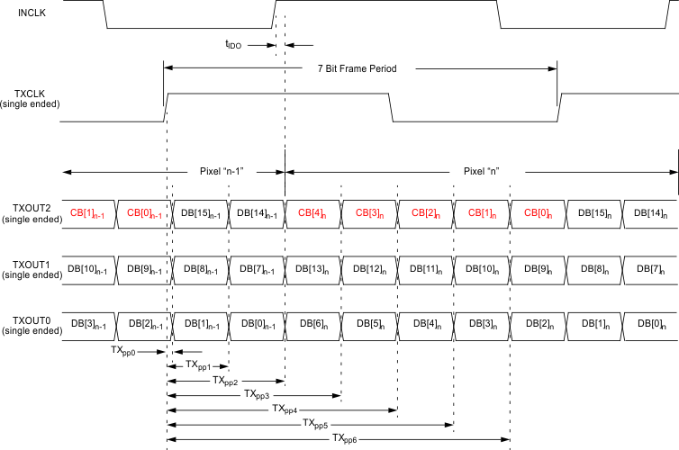 Figure 49. LVDS Data Output Mode Specification Diagram
7.4.20.1 Optional TXCLK Delay
The LM98722 includes a selectable (off by default) delay of TXCLK. This delay can be enabled (Page 8, Register 0x08, Bit 3) to improve timing margin between the TXCLK and TXOUTx signals when using certain LVDS deserializers. The default/off setting is intended to be compatible with the LM98714 LVDS timing.
7.4.21 LVDS Data Latency Diagrams
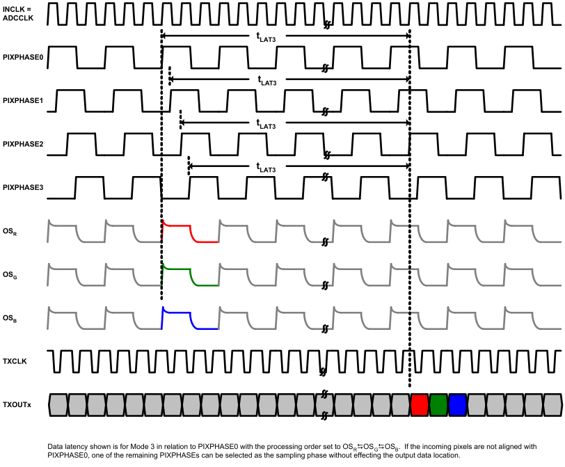 Figure 50. Mode 3 LVDS Data Latency
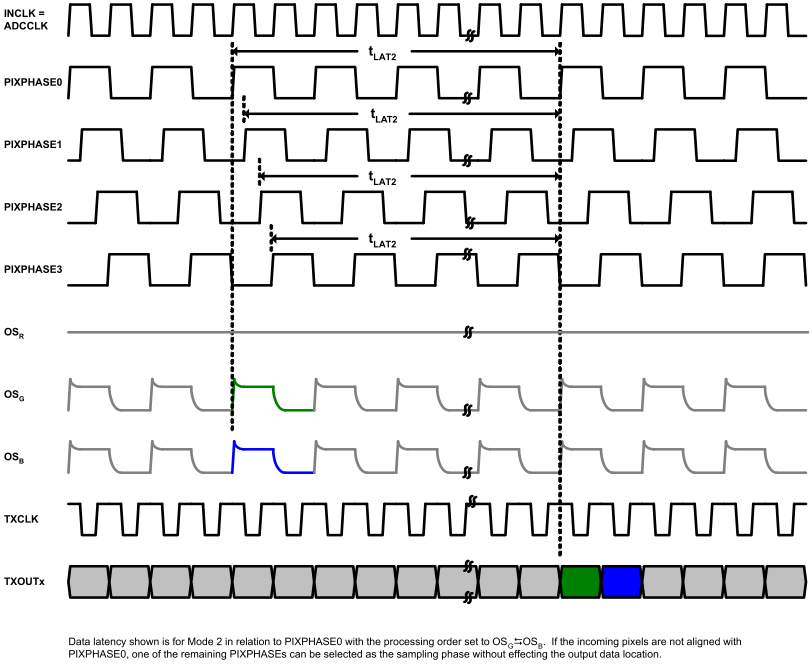 Figure 51. Mode 2 LVDS Data Latency
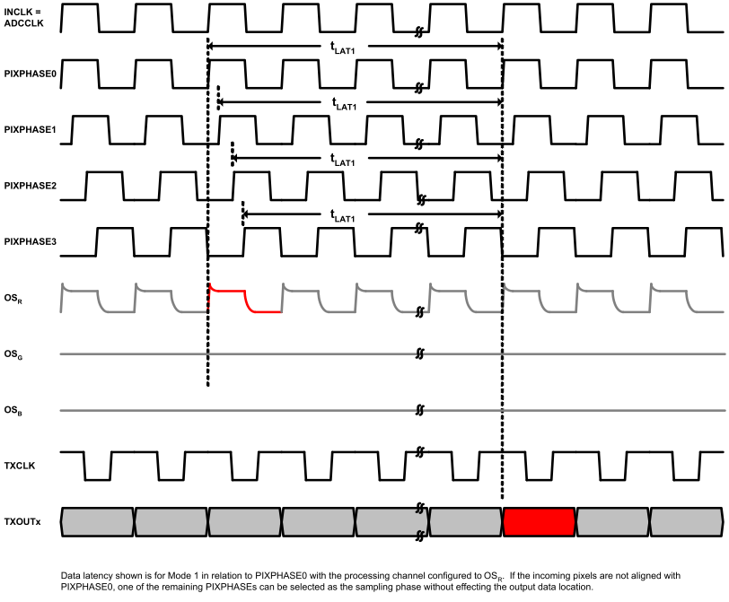 Figure 52. Mode 1 LVDS Data Latency
7.4.22 Data Test Patterns
The data test patterns present different data to the input of the LVDS serializer block. There are two basic groups of test patterns:
- LVDS Output Pattern Modes - These patterns are applicable to all 21 bits of the LVDS interface.
- AFE Output Pattern Modes (Default) - These patterns are applicable to the 16 bit AFE data sent to the LVDS interface.
- All Test Pattern Modes are selected at Page 0, Register 6.
7.4.22.1 LVDS Output Pattern Modes
7.4.22.1.1 Worst Case Transitions (Alternating 0x2A/0x55 on Each LVDS Pair)
This test mode provides an LVDS output with the maximum possible transitions. This mode is useful for system EMI evaluations, and for ATE timing tests.
The effective data values are an alternating pattern between 21’b101010101010101010101 (0x155555) and 21’b010101010101010101010 (0x0AAAAA). This test pattern resets to 0x155555 at the selected event (BOL or BOS).
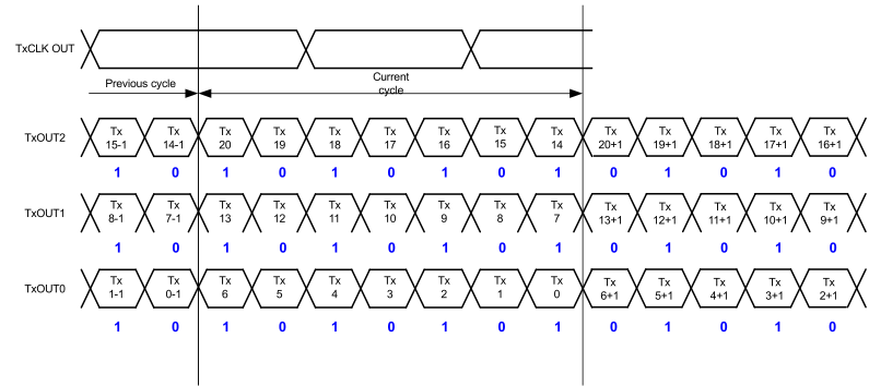 Figure 53. Worst Case Transitions (Alternating 0x2A/0x55 on Each LVDS Pair)
7.4.22.1.2 Fixed Output Data
This mode sends a fixed repeating data pattern to each of the indicated LVDS output pairs. This is useful for system debugging of the LVDS link and receiver circuitry. There are 4 different choices within this mode:
- 0x2A (0101010b) (All 3 data pairs)
- 0x55 (1010101b) (All 3 data pairs)
- 0x00 (0000000b) (*All 3 data pairs + clock pair)
- 0x7F (1111111b) (*All 3 data pairs + clock pair)
*Since the 0x00 and 0x7F patterns also affect the clock pair, they cannot be used for deserializer and downstream testing. They are useful for DC measurements of the LVDS outputs.
7.4.22.2 AFE Output Pattern Modes
There are 3 different types of AFE Output Patterns:
- Normal ADC/AFE output (Default)
- Up-Counter Data
- Fixed AFE Patterns
Up-Counter Data
The counter will be reset to 0xFFFF during the BOS (Beginning Of Scan) SH Interval. When the AFE up-counter is selected, the ramp begins at the BOS, and increments by 1 at either the pixel rate or at the line rate (every BOL). This data can be useful as it can provide a grayscale image that increases in intensity down the “page”. Alternately, it can provide data that increments at the pixel rate. Either of these forms can be very useful in debugging the downstream data processing system.
Fixed AFE Pattern
The fixed AFE patterns allow the CB coding information to be sent normally, while specific data is used to replace the AFE output. This can be useful in debugging portions of the downstream data processing system.
- 0xFF00 (0x1111111100000000b) fixed data
- 0xAA55 (0x1010101001010101b) fixed data
- 0x0000 (0x0000000000000000b) fixed data
- 0xFFFF (0x1111111111111111b) fixed data
- 0x00FF (0x0000000011111111b) fixed data
- 0x55AA (0x0101010110101010b) fixed data
7.4.23 CMOS Output Format
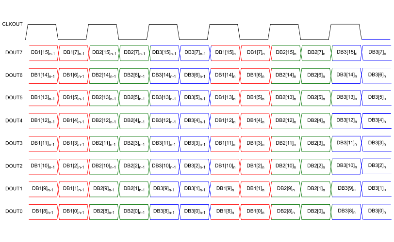 Figure 54. CMOS Data Output Format (Mode 3 Shown)
7.4.24 CMOS Output Data Latency Diagrams
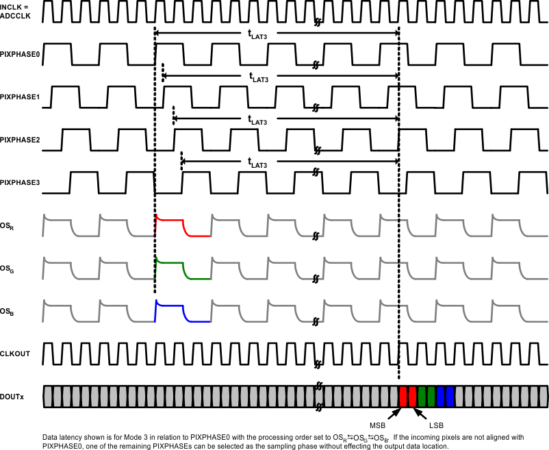 Figure 55. Mode 3 CMOS Output Latency
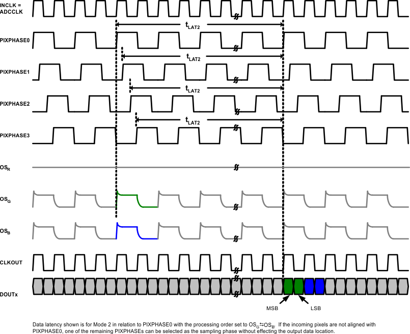 Figure 56. Mode 2 CMOS Output Latency
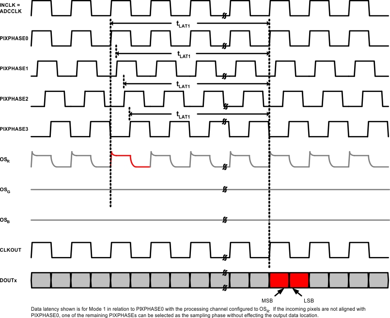 Figure 57. Mode 1 CMOS Output Latency
7.4.25 Serial Interface
A serial interface is used to write and read the configuration registers. The interface is a four wire interface using SCLK, SEN, SDI and SDO connections. SDI and SDO can be connected together to support the same format and connectivity as previous LM98714 designs. The CE pin should be tied to GND to support LM98714 compatible communications. This will set the device address bits to 00.
Table 15. Serial Interface "CE" Pin Definition
| CE LEVEL | ADDRESS |
|---|---|
| VD | 01 |
| Float | 10 |
| GND | 00 |
The main input clock (INCLK) to the LM98722 can be active or stopped when accessing the Serial Interface. Care should be taken to avoid stopping or starting the INCLK during Serial Interface communication.
NOTE
After either starting or stopping INCLK, or after Software Reset (Register Page 0, Address 1, [4:3]), users should wait for 50 ms to allow the internal PLL and logic to stabilize before resuming Serial Interface communications.
7.4.25.1 Serial Interface Operating Modes
- LM98714 Compatible Mode (Default): By default the serial interface is compatible with the LM98714 interface, allowing SDI and SDO to be connected and driving by a single pin on the host.
- LM98722 4 Wire 16+ Clock Mode (Default): The 4 Wire 16+ Clock Mode is essentially the same as the LM98714 Compatible Mode, but using all 4 wires, with separate SDO and SDI signals between the Host and Slave. This requires additional wires, but removes the need for a bidirectional signal. A valid transaction is recognized after a minimum of 16 SCLK while SEN is low.
- LM98722 25+ Clock Mode (Selected when Page 0, Register 0x01h, Bit 7=1: This mode forces the serial interface logic to only process a transaction with 25 or more SCLK while SEN is low. This mode can be used with either 3 or 4 wire connections. In all of the above cases, the final 16 bits on SDI (before the rising edge of SEN) are processed by the serial interface logic. Any earlier information on SDI is ignored.
- Serial Interface in Absence of MCLK
- Clockless (MCLK stopped) Mode (always enabled if MCLK stopped): When the input MCLK is stopped, Data Read operation is exactly the same as MCLK present mode. The Data Write operation no longer provides a free readback of the previously written data. See Figure 60 and Figure 63.
7.4.25.2 Serial Interface in Absence of MCLK
Clockless (MCLK stopped) Mode (always enabled if MCLK stopped) - When the input MCLK is stopped, Data Read operation is exactly the same as MCLK present mode. The Data Write operation no longer provides a free readback of the previously written data. See Figure 60 and Figure 62.
7.4.25.3 Writing to the Serial Registers
To write to the serial registers, the timing diagram shown in Figure 58 must be met. First, SEN is toggled low. The *previously addressed device assumes control of the SDO pin during the first eight clocks of the command. During this period, data is clocked out of the device at the rising edge of SCLK. At the rising edge of ninth clock, the LM98722 releases control of the SDO pin. At the falling edge of the ninth clock period, the master should assume control of the SDI pin and begin issuing the new command. SDI is clocked into the LM98722 at the rising edge of SCLK. The remaining bits are composed of the “write” command bit (a zero), two device address bits (00, 01 or 10 for the LM98722), five bit register address to be written, and the eight bit register value to be written. When SEN toggles high, the register is written to, and the LM98722 now functions with this new data.
The previously addressed device could be another device on a shared serial interface or this device. If the previous command was to this device, and was a read, then the SDO pin will be driven during the first eight clocks. If the previous command was to this device and was a write, then the SDO pin will only be driven if the serial interface is in “MCLK active” mode.
7.4.25.4 Reading The Serial Registers
To read to the serial registers, the timing diagram shown Figure 59 must be met. First, SEN is toggled low. The LM98722 assumes control of the SDO pin during the first eight clocks of the command. During this period, data is clocked out of the device at the rising edge of SCLK. The eight bit value clocked out is the contents of the previously addressed register, regardless if the previous command was a read or a write. At the rising edge of ninth clock, the LM98722 releases control of the SDO pin. At the falling edge of the ninth clock period, the master should assume control of the SDI pin and begin issuing the new command. SDI is clocked into the LM98722 at the rising edge of SCLK. The remaining bits are composed of the “read” command bit (a one), two device address bits (zeros for the LM98722), five bit register address to be read, and the eight bit “don’t care” bits. When SEN toggles high, the register is not written to, but its contents are staged to be outputted at the beginning of the next command.
Examples of Serial Writes and Reads in the various modes are shown in Figure 58 through Figure 64.
7.4.25.5 LM98714 Compatible 3 Wire Serial Signaling
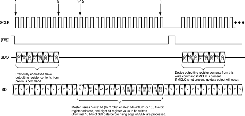 Figure 58. Serial Write - LM98714 Compatible Connection
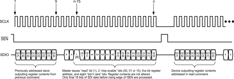 Figure 59. Serial Read - LM98714 Compatible Connection
7.4.25.6 LM98722 4 Wire Serial Signaling
 Figure 60. Serial Write - 4 Wire Connection - 25+ Clock Mode
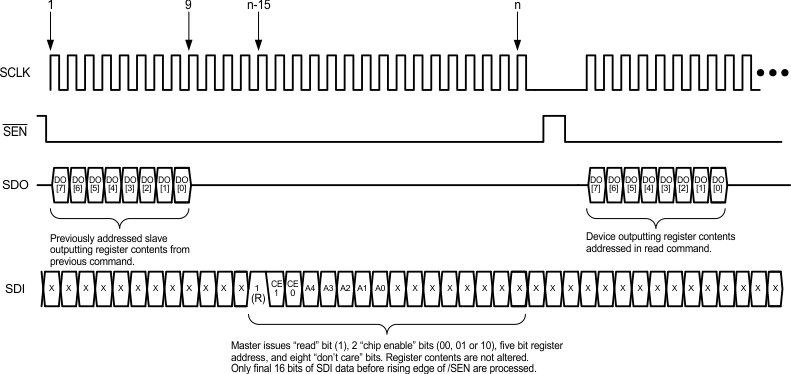 Figure 61. Serial Read - 4 Wire Connection - 25+ Clock Mode
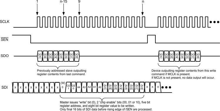 Figure 62. Serial Write - 4 Wire Connection - 16+ Clock Mode
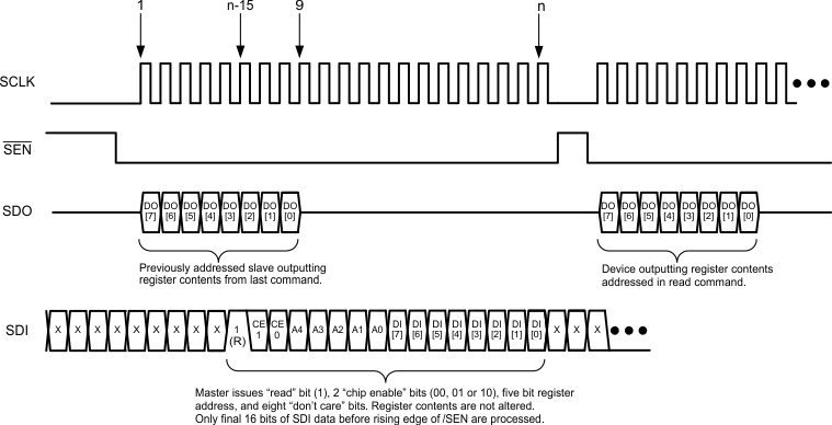 Figure 63. Serial Read - 4 Wire Connection - 16+ Clock Mode
7.4.25.7 Serial Interface Timing Details
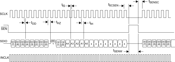 Figure 64. Serial Interface Specification Diagram
7.5 Registers Maps
7.5.1 Configuration Registers
The LM98722 operation is very flexible to support a wide variety of sensors and system designs. This flexibility is controlled through configuration registers which are first summarized, then described in full in the register tables. Because the serial interface only allows 5 address bits, a register paging system is used to support the larger number of required registers.
The page register is present at the highest address (1Fh or 11111b) of the currently selected page. The power on default setting of the page register is 00. Writing other values to this register allows the other pages to be accessed.
Once all registers are written, the Register Lock Control bit (Page 0, Register 0, Bit 0) is set to 1 to start the state machines and initiate the converting of pixels. If Slave mode is selected, SH_R pulses must also be input to trigger this process.
NOTE
When Register Lock Control = 1, many registers are locked to prevent state machines from becoming corrupted, while others are accessible to allow control of necessary functions. The registers and bits that are still writable are indicated in Boldface print in the Bits and Register Description columns of the Register Definition Details table.
Operational Setup Sequence:
Ensure Lock Bit (Page 0, Register 0, Bit 0) = 0 for following setting writes
Apply either no INCLK or a stable INCLK to ensure accurate serial communications
Page 0
- Set AFE mode (# of input channels)
- Set output data format
- Enable data outputs
- Set AFE biasing
- Set AFE Clamp and Sample timing
- Setup Slave or Master Mode
Page 1
- Set Gain Mode (Single or Dual)
- Set CDS/SH Gain
- Set PGA
- Set DAC settings
Page 2
- Set Input Clamping Settings
- Set Black Pixel Start and # Black Pixels Averaged
- Set Active White Pixels Start and End
- Set Line Length (Master Mode Only)
- Set # Pixel Multiplier, SH Line Sequence # and SH State Length Multiplier
- Set PHI, RS, CP On and Off delay settings
- Set Spread Spectrum control settings
Page 3
- Set SH State Length settings
Page 4
- Set SH Interval State Settings for PHI, RS, CP
Page 5
- Set SH Interval State Settings for SH1 to SH5
Page 6
- Set PHI, RS, CP pattern bit fields and rate (normal or 1/2 rate)
Page 7
- Set SHx On, Off settings if needed
- Set CLK invert settings for multi-line sequences if needed
Page 8
- Set CLK output activity, polarity, enable
- Set LVDS output format
- Set CB coding
- Set PHI, RS, CP, SH unlock output state
Begin Scanning:
- Ensure stable INCLK applied and PLL is locked (read back Page 0, Register 0, Bit 7)
- Set Register Lock Control bit = 1
- In Master Mode, conversions will begin after the Lock Bit is set. In Slave Mode, SH_R pulses can begin after the Lock Bit is set. SH Intervals will be generated in response to the SH_R input pulses.
- Registers and Bits marked in Boldface print may be adjusted while scanning is in progress. More major changes (i.e.: color mode, CCDTG details) should be done by writing a 0 to the Register Lock Control Bit to pause scanning.
Table 16. Register Summary Table
| PAGE (dec) |
ADDR (dec) |
ADDR (hex) |
DEFAULT (binary) |
REGISTER TITLE |
|---|---|---|---|---|
| PAGE 0 | ||||
| 0 | 0 | 0 | 0010 0000 | Main Configuration 0 |
| 0 | 1 | 1 | 0100 0000 | Main Configuration 1 |
| 0 | 2 | 2 | 1100 0000 | Main Configuration 2 |
| 0 | 3 | 3 | 1000 0010 | Main Configuration 3 |
| 0 | 4 | 4 | 0011 0000 | Main Configuration 4 |
| 0 | 5 | 5 | 0000 0000 | Main Configuration 5 |
| 0 | 6 | 6 | 0000 0000 | Configuration 6 |
| 0 | 7 | 7 | 0000 0000 | Configuration 7 |
| 0 | 8 | 8 | 0000 0000 | OSR CLAMP Start Edge |
| 0 | 9 | 9 | 0001 0000 | OSR CLAMP Stop Edge |
| 0 | 10 | A | 0000 0000 | OSG CLAMP Start Edge |
| 0 | 11 | B | 0001 0000 | OSG CLAMP Stop Edge |
| 0 | 12 | C | 0000 0000 | OSB CLAMP Start Edge |
| 0 | 13 | D | 0001 0000 | OSB CLAMP Stop Edge |
| 0 | 14 | E | 0001 0110 | OSR SAMPLE Start Edge |
| 0 | 15 | F | 0010 0110 | OSR SAMPLE Stop Edge |
| 0 | 16 | 10 | 0001 0110 | OSG SAMPLE Start Edge |
| 0 | 17 | 11 | 0010 0110 | OSG SAMPLE Stop Edge |
| 0 | 18 | 12 | 0001 0110 | OSB SAMPLE Start Edge |
| 0 | 19 | 13 | 0010 0110 | OSB SAMPLE Stop Edge |
| 0 | 20 | 14 | 0000 0000 | Sample & Clamp Monitor 0 |
| 0 | 21 | 15 | 0000 0000 | Sample & Clamp Monitor 1 |
| 0 | 22 to 29 | 16 to 1D | Reserved | |
| 0 | 30 | 1E | XX00 0011 | Revision |
| 0 | 31 | 1F | 0000 0000 | Page Register |
| PAGE 1 | ||||
| 1 | 0 | 0 | 0000 0000 | Gain Mode |
| 1 | 1 | 1 | 0110 0001 | Red PGA |
| 1 | 2 | 2 | 0110 0001 | Green PGA |
| 1 | 3 | 3 | 0110 0001 | Blue PGA |
| 1 | 4 | 4 | 1000 0000 | Red Even DAC MSB |
| 1 | 5 | 5 | 0000 0000 | Red Even DAC LSB |
| 1 | 6 | 6 | 1000 0000 | Green Even DAC MSB |
| 1 | 7 | 7 | 0000 0000 | Green Even DAC LSB |
| 1 | 8 | 8 | 1000 0000 | Blue Even DAC MSB |
| 1 | 9 | 9 | 0000 0000 | Blue Even DAC LSB |
| 1 | 10 | A | 1000 0000 | Red Odd DAC MSB |
| 1 | 11 | B | 0000 0000 | Red Odd DAC LSB |
| 1 | 12 | C | 1000 0000 | Green Odd DAC MSB |
| 1 | 13 | D | 0000 0000 | Green Odd DAC LSB |
| 1 | 14 | E | 1000 0000 | Blue Odd DAC MSB |
| 1 | 15 | F | 0000 0000 | Blue Odd DAC LSB |
| 1 | 16 | 10 | 0100 0000 | Red Even Digital Offset |
| 1 | 17 | 11 | 0100 0000 | Green Even Digital Offset |
| 1 | 18 | 12 | 0100 0000 | Blue Even Digital Offset |
| 1 | 19 | 13 | 0100 0000 | Red Odd Digital Offset |
| 1 | 20 | 14 | 0100 0000 | Green Odd Digital Offset |
| 1 | 21 | 15 | 0100 0000 | Blue Odd Digital Offset |
| 1 | 22 | 16 | 0110 0001 | Red High Gain PGA |
| 1 | 23 | 17 | 0110 0001 | Green High Gain PGA |
| 1 | 24 | 18 | 0110 0001 | Blue High Gain PGA |
| 1 | 28 | 1C | 0100 0000 | Red Channel Bimodal |
| 1 | 29 | 1D | 0100 0000 | Green Channel Bimodal |
| 1 | 30 | 1E | 0100 0000 | Blue Channel Bimodal |
| 1 | 31 | 1F | 0000 0000 | Page Register |
| PAGE 2 | ||||
| 2 | 0 | 0 | 0000 0000 | Calibration Mode |
| 2 | 1 | 1 | 0000 0000 | Calibration # Lines |
| 2 | 2 | 2 | 0001 0100 | Black Cal Config |
| 2 | 3 | 3 | 0100 0000 | Black Target |
| 2 | 4 | 4 | 0100 0011 | White Cal Config |
| 2 | 5 | 5 | 1000 0000 | White Target |
| 2 | 6 | 6 | 0000 0100 | AutoCLPIN Start |
| 2 | 7 | 7 | 0000 1100 | AutoCLPIN End |
| 2 | 8 | 8 | 0001 0000 | Black Loop Start |
| 2 | 9 | 9 | 0000 0000 | Active/White Pixels Start - MSB |
| 2 | 10 | A | 0001 0100 | Active/White Pixels Start - LSB |
| 2 | 11 | B | 0001 0000 | Active/White Pixels End - MSB |
| 2 | 12 | C | 0000 0000 | Active/White Pixels End - LSB |
| 2 | 13 | D | 0001 0000 | Line Length MSB |
| 2 | 14 | E | 0100 0000 | Line Length LSB |
| 2 | 15 | F | 0000 0000 | Line Length Multiplier |
| 2 | 16 | 10 | 0000 0000 | Line Mode |
| 2 | 17 | 11 | 0000 0000 | SH State Length Multiplier |
| 2 | 18 | 12 | 0000 0000 | PHIA/B/C Delays |
| 2 | 19 | 13 | 0000 0000 | RS/CP Delays |
| 2 | 20 to 23 | 14 to 17 | Reserved | |
| 2 | 24 | 18 | 1111 1000 | PLL Control 1 |
| 2 | 25 | 19 | 0001 1000 | PLL Control 2 |
| 2 | 26 | 1A | 0000 0000 | SSCG Control 1 |
| 2 | 27 | 1B | 0000 0010 | SSCG Control 2 |
| 2 | 28 | 1C | 0000 0000 | Clock Mult M |
| 2 | 29 | 1D | 0000 0000 | Clock Mult N |
| 2 | 30 | 1E | 0000 0000 | SSCG Control 3 |
| 2 | 31 | 1F | Page Register | |
| PAGE 3 | ||||
| 3 | 0 | 0 | 0000 0000 | SH State 0 Length |
| 3 | 1 | 1 | 0000 0000 | SH State 1 Length |
| 3 | 2 | 2 | 0000 0000 | SH State 2 Length |
| 3 | 3 | 3 | 0000 0000 | SH State 3 Length |
| 3 | 4 | 4 | 0000 0000 | SH State 4 Length |
| 3 | 5 | 5 | 0000 0000 | SH State 5 Length |
| 3 | 6 | 6 | 0000 0000 | SH State 6 Length |
| 3 | 7 | 7 | 0000 0000 | SH State 7 Length |
| 3 | 8 | 8 | 0000 0000 | SH State 8 Length |
| 3 | 9 | 9 | 0000 0000 | SH State 9 Length |
| 3 | 10 | A | 0000 0000 | SH State 10 Length |
| 3 | 11 | B | 0000 0000 | SH State 11 Length |
| 3 | 12 | C | 0000 0000 | SH State 12 Length |
| 3 | 13 | D | 0000 0000 | SH State 13 Length |
| 3 | 14 | E | 0000 0000 | SH State 14 Length |
| 3 | 15 | F | 0000 0000 | SH State 15 Length |
| 3 | 16 | 10 | 0000 0000 | SH State 16 Length |
| 3 | 17 | 11 | 0000 0000 | SH State 17 Length |
| 3 | 18 | 12 | 0000 0000 | SH State 18 Length |
| 3 | 19 | 13 | 0000 0000 | SH State 19 Length |
| 3 | 20 | 14 | 0000 0000 | SH State 20 Length |
| 3 | 21 | 15 | 0000 0000 | SH State 21 Length |
| 3 | 22 | 16 | 0000 0000 | SH State 22 Length |
| 3 | 23 | 17 | 0000 0000 | SH State 23 Length |
| 3 | 24 | 18 | 0000 0000 | SH State 24 Length |
| 3 | 25 | 19 | 0000 0000 | SH State 25 Length |
| 3 | 26 | 1A | 0000 0000 | SH State 26 Length |
| 3 | 27 | 1B | 0000 0000 | SH State 27 Length |
| 3 | 28 | 1C | 0000 0000 | SH State 28 Length |
| 3 | 29 | 1D | 0000 0000 | SH State 29 Length |
| 3 | 30 | 1E | 0000 0000 | SH State 30 Length |
| 3 | 31 | 1F | Page Register | |
| PAGE 4 | ||||
| 4 | 0 | 0 | 0000 0000 | SH State 0 PHI, RS, CP |
| 4 | 1 | 1 | 0000 0000 | SH State 1 PHI, RS, CP |
| 4 | 2 | 2 | 0000 0000 | SH State 2 PHI, RS, CP |
| 4 | 3 | 3 | 0000 0000 | SH State 3 PHI, RS, CP |
| 4 | 4 | 4 | 0000 0000 | SH State 4 PHI, RS, CP |
| 4 | 5 | 5 | 0000 0000 | SH State 5 PHI, RS, CP |
| 4 | 6 | 6 | 0000 0000 | SH State 6 PHI, RS, CP |
| 4 | 7 | 7 | 0000 0000 | SH State 7 PHI, RS, CP |
| 4 | 8 | 8 | 0000 0000 | SH State 8 PHI, RS, CP |
| 4 | 9 | 9 | 0000 0000 | SH State 9 PHI, RS, CP |
| 4 | 10 | A | 0000 0000 | SH State 10 PHI, RS, CP |
| 4 | 11 | B | 0000 0000 | SH State 11 PHI, RS, CP |
| 4 | 12 | C | 0000 0000 | SH State 12 PHI, RS, CP |
| 4 | 13 | D | 0000 0000 | SH State 13 PHI, RS, CP |
| 4 | 14 | E | 0000 0000 | SH State 14 PHI, RS, CP |
| 4 | 15 | F | 0000 0000 | SH State 15 PHI, RS, CP |
| 4 | 16 | 10 | 0000 0000 | SH State 16 PHI, RS, CP |
| 4 | 17 | 11 | 0000 0000 | SH State 17 PHI, RS, CP |
| 4 | 18 | 12 | 0000 0000 | SH State 18 PHI, RS, CP |
| 4 | 19 | 13 | 0000 0000 | SH State 19 PHI, RS, CP |
| 4 | 20 | 14 | 0000 0000 | SH State 20 PHI, RS, CP |
| 4 | 21 | 15 | 0000 0000 | SH State 21 PHI, RS, CP |
| 4 | 22 | 16 | 0000 0000 | SH State 22 PHI, RS, CP |
| 4 | 23 | 17 | 0000 0000 | SH State 23 PHI, RS, CP |
| 4 | 24 | 18 | 0000 0000 | SH State 24 PHI, RS, CP |
| 4 | 25 | 19 | 0000 0000 | SH State 25 PHI, RS, CP |
| 4 | 26 | 1A | 0000 0000 | SH State 26 PHI, RS, CP |
| 4 | 27 | 1B | 0000 0000 | SH State 27 PHI, RS, CP |
| 4 | 28 | 1C | 0000 0000 | SH State 28 PHI, RS, CP |
| 4 | 29 | 1D | 0000 0000 | SH State 29 PHI, RS, CP |
| 4 | 30 | 1E | 0000 0000 | SH State 30 PHI, RS, CP |
| 4 | 31 | 1F | Page Register | |
| PAGE 5 | ||||
| 5 | 0 | 0 | 0000 0000 | SH State 0 SH1-SH5 |
| 5 | 1 | 1 | 0000 0000 | SH State 1 SH1-SH5 |
| 5 | 2 | 2 | 0000 0000 | SH State 2 SH1-SH5 |
| 5 | 3 | 3 | 0000 0000 | SH State 3 SH1-SH5 |
| 5 | 4 | 4 | 0000 0000 | SH State 4 SH1-SH5 |
| 5 | 5 | 5 | 0000 0000 | SH State 5 SH1-SH5 |
| 5 | 6 | 6 | 0000 0000 | SH State 6 SH1-SH5 |
| 5 | 7 | 7 | 0000 0000 | SH State 7 SH1-SH5 |
| 5 | 8 | 8 | 0000 0000 | SH State 8 SH1-SH5 |
| 5 | 9 | 9 | 0000 0000 | SH State 9 SH1-SH5 |
| 5 | 10 | A | 0000 0000 | SH State 10 SH1-SH5 |
| 5 | 11 | B | 0000 0000 | SH State 11 SH1-SH5 |
| 5 | 12 | C | 0000 0000 | SH State 12 SH1-SH5 |
| 5 | 13 | D | 0000 0000 | SH State 13 SH1-SH5 |
| 5 | 14 | E | 0000 0000 | SH State 14 SH1-SH5 |
| 5 | 15 | F | 0000 0000 | SH State 15 SH1-SH5 |
| 5 | 16 | 10 | 0000 0000 | SH State 16 SH1-SH5 |
| 5 | 17 | 11 | 0000 0000 | SH State 17 SH1-SH5 |
| 5 | 18 | 12 | 0000 0000 | SH State 18 SH1-SH5 |
| 5 | 19 | 13 | 0000 0000 | SH State 19 SH1-SH5 |
| 5 | 20 | 14 | 0000 0000 | SH State 20 SH1-SH5 |
| 5 | 21 | 15 | 0000 0000 | SH State 21 SH1-SH5 |
| 5 | 22 | 16 | 0000 0000 | SH State 22 SH1-SH5 |
| 5 | 23 | 17 | 0000 0000 | SH State 23 SH1-SH5 |
| 5 | 24 | 18 | 0000 0000 | SH State 24 SH1-SH5 |
| 5 | 25 | 19 | 0000 0000 | SH State 25 SH1-SH5 |
| 5 | 26 | 1A | 0000 0000 | SH State 26 SH1-SH5 |
| 5 | 27 | 1B | 0000 0000 | SH State 27 SH1-SH5 |
| 5 | 28 | 1C | 0000 0000 | SH State 28 SH1-SH5 |
| 5 | 29 | 1D | 0000 0000 | SH State 29 SH1-SH5 |
| 5 | 30 | 1E | 0000 0000 | SH State 30 SH1-SH5 |
| 5 | 31 | 1F | Page Register | |
| PAGE 6 | ||||
| 6 | 0 | 0 | 0000 0000 | PHIA0 |
| 6 | 1 | 1 | 0000 0000 | PHIA1 |
| 6 | 2 | 2 | 0000 0000 | PHIA2 |
| 6 | 3 | 3 | 0000 0000 | PHIA3 |
| 6 | 4 | 4 | 0000 0000 | PHIA4 |
| 6 | 5 | 5 | 0000 0000 | PHIA5 |
| 6 | 6 | 6 | 0000 0000 | PHIB0 |
| 6 | 7 | 7 | 0000 0000 | PHIB1 |
| 6 | 8 | 8 | 0000 0000 | PHIB2 |
| 6 | 9 | 9 | 0000 0000 | PHIB3 |
| 6 | 10 | A | 0000 0000 | PHIB4 |
| 6 | 11 | B | 0000 0000 | PHIB5 |
| 6 | 12 | C | 0000 0000 | PHIC0 |
| 6 | 13 | D | 0000 0000 | PHIC1 |
| 6 | 14 | E | 0000 0000 | PHIC2 |
| 6 | 15 | F | 0000 0000 | PHIC3 |
| 6 | 16 | 10 | 0000 0000 | PHIC4 |
| 6 | 17 | 11 | 0000 0000 | PHIC5 |
| 6 | 18 | 12 | 0000 0000 | RS0 |
| 6 | 19 | 13 | 0000 0000 | RS1 |
| 6 | 20 | 14 | 0000 0000 | RS2 |
| 6 | 21 | 15 | 0000 0000 | RS3 |
| 6 | 22 | 16 | 0000 0000 | RS4 |
| 6 | 23 | 17 | 0000 0000 | RS5 |
| 6 | 24 | 18 | 0000 0000 | CP0 |
| 6 | 25 | 19 | 0000 0000 | CP1 |
| 6 | 26 | 1A | 0000 0000 | CP2 |
| 6 | 27 | 1B | 0000 0000 | CP3 |
| 6 | 28 | 1C | 0000 0000 | CP4 |
| 6 | 29 | 1D | 0000 0000 | CP5 |
| 6 | 30 | 1E | 0000 0000 | HSPIX Rate Select |
| 6 | 31 | 1F | Page Register | |
| PAGE 7 | ||||
| 7 | 0 | 0 | 0000 0000 | SH1 PIXEL ON MSB |
| 7 | 1 | 1 | 0000 0000 | SH1 PIXEL ON LSB |
| 7 | 2 | 2 | 0000 0000 | SH1 PIXEL OFF MSB |
| 7 | 3 | 3 | 0000 0000 | SH1 PIXEL OFF LSB |
| 7 | 4 | 4 | 0000 0000 | SH2 PIXEL ON MSB |
| 7 | 5 | 5 | 0000 0000 | SH2 PIXEL ON LSB |
| 7 | 6 | 6 | 0000 0000 | SH2 PIXEL OFF MSB |
| 7 | 7 | 7 | 0000 0000 | SH2 PIXEL OFF LSB |
| 7 | 8 | 8 | 0000 0000 | SH3 PIXEL ON MSB |
| 7 | 9 | 9 | 0000 0000 | SH3 PIXEL ON LSB |
| 7 | 10 | A | 0000 0000 | SH3 PIXEL OFF MSB |
| 7 | 11 | B | 0000 0000 | SH3 PIXEL OFF LSB |
| 7 | 12 | C | 0000 0000 | SH4 PIXEL ON MSB |
| 7 | 13 | D | 0000 0000 | SH4 PIXEL ON LSB |
| 7 | 14 | E | 0000 0000 | SH4 PIXEL OFF MSB |
| 7 | 15 | F | 0000 0000 | SH4 PIXEL OFF LSB |
| 7 | 16 | 10 | 0000 0000 | SH5 PIXEL ON MSB |
| 7 | 17 | 11 | 0000 0000 | SH5 PIXEL ON LSB |
| 7 | 18 | 12 | 0000 0000 | SH5 PIXEL OFF MSB |
| 7 | 19 | 13 | 0000 0000 | SH5 PIXEL OFF LSB |
| 7 | 20 | 14 | 0000 0000 | PHIA Polarity Override |
| 7 | 21 | 15 | 0000 0000 | PHIB Polarity Override |
| 7 | 22 | 16 | 0000 0000 | PHIC Polarity Override |
| 7 | 23 | 17 | 0000 0000 | RS Polarity Override |
| 7 | 24 | 18 | 0000 0000 | CP Polarity Override |
| 7 | 25 | 19 | 0000 0000 | SH1 Polarity Override |
| 7 | 26 | 1A | 0000 0000 | SH2 Polarity Override |
| 7 | 27 | 1B | 0000 0000 | SH3 Polarity Override |
| 7 | 28 | 1C | 0000 0000 | SH4 Polarity Override |
| 7 | 29 | 1D | 0000 0000 | SH5 Polarity Override |
| 7 | 30 | 1E | 0000 0000 | Reserved |
| 7 | 31 | 1F | Page Register | |
| PAGE 8 | ||||
| 8 | 0 | 0 | 0000 0000 | PHIA1, PHIA2 Polarity / State |
| 8 | 1 | 1 | 0000 0000 | PHIB1, PHIB2 Polarity / State |
| 8 | 2 | 2 | 0000 0000 | PHIC1, PHIC2 Polarity / State |
| 8 | 3 | 3 | 0000 0000 | RS, CP Polarity / State |
| 8 | 4 | 4 | 0000 0000 | SH1, SH2 Polarity / State |
| 8 | 5 | 5 | 0000 0000 | SH3, SH4 Polarity / State |
| 8 | 6 | 6 | 0000 0000 | SH5 Polarity / State |
| 8 | 7 | 7 | 0000 0000 | Reserved |
| 8 | 8 | 8 | 0010 0000 | LVDS Configuration |
| 8 | 9 | 9 | 0000 0000 | CB1/CB0 CB Mapping |
| 8 | 10 | A | 0000 0000 | CB3/CB2 CB Mapping |
| 8 | 11 | B | 0000 0000 | D2/CB4 CB Mapping |
| 8 | 12 | C | 0000 0000 | D4/D3 CB Mapping |
| 8 | 13 | D | 0000 0000 | D5 CB Mapping |
| 8 | 14 | E | 0000 0000 | Unlock State Output Values PHIA, PHIB, PHIC, RS, CP |
| 8 | 15 | F | 0000 0000 | Unlock State Output Values SH1, SH2, SH3, SH4, SH5 |
| 8 | 16 to 17 | 10 to 11 | 0000 0000 | Reserved |
| 8 | 18 | 12 | 0000 0000 | Scrambler Inhibit 0 (LVDS[6:0]) |
| 8 | 19 | 13 | 0000 0000 | Scrambler Inhibit 1 (LVDS[13:7]) |
| 8 | 20 | 14 | 0000 0000 | Scrambler Inhibit 2 (LVDS[20:14]) |
| 8 | 16 to 30 | 15 to 1E | 0000 0000 | Reserved |
| 8 | 31 | 1F | Page Register | |
The following section describes all available registers in the LM98722 register bank, and their functions.
***Registers and/or Bits Marked in Boldface are Writeable when Register 0, Bit 0 = 1, all others are “Locked”.***
Table 17. Register Definition, Page 0
Table 18. Register Definition, Page 1
| PAGE (dec) |
ADDR (dec) |
ADDR (hex) |
DEFAULT (binary) |
BITS |
REGISTER TITLE |
REGISTER DESCRIPTION |
|---|---|---|---|---|---|---|
| 1 | 0 | 0 | 0000 0000 | [7] | Gain Mode | CDS/SH Gain Blue - 0 = 1x Gain, 1 = 2x Gain |
| [6] | CDS/SH Gain Green - 0 = 1x Gain, 1 = 2x Gain | |||||
| [5] | CDS/SH Gain Blue - 0 = 1x Gain, 1 = 2x Gain | |||||
| [4:3] | Not used | |||||
| [2] | Individual CDS/SH Gain Enable | |||||
| 0 Use Bit 0 for CDS/SH Gain | ||||||
| 1 Use Bits 7:5 for CDS/SH Gains | ||||||
| [1] | Dual Gain Mode Enable | |||||
| 0 Single Gain Setting Within Each Line | ||||||
| 1 Two Gain Settings Within Each Line | ||||||
| [0] | Gain Select | |||||
| 0 1x CDS/SH Gain - Default | ||||||
| 1 2x CDS/SH Gain | ||||||
| 1 | 1 | 1 | 0110 0001 | [7:0] | Red PGA | Default = 97d for Gain = 1 |
| 1 | 2 | 2 | 0110 0001 | [7:0] | Green PGA | Default = 97d for Gain = 1 |
| 1 | 3 | 3 | 0110 0001 | [7:0] | Blue PGA | Default = 97d for Gain = 1 |
| 1 | 4 | 4 | 1000 0000 | [7:0] | Red Even DAC MSB | DAC[9:2] |
| 1 | 5 | 5 | 0000 0000 | [7:2] | Red Even DAC LSB | Not Used |
| [1:0] | DAC[1:0] | |||||
| 1 | 6 | 6 | 1000 0000 | [7:0] | Green Even DAC MSB | DAC[9:2] |
| 1 | 7 | 7 | 0000 0000 | [7:2] | Green Even DAC LSB | Not Used |
| [1:0] | DAC[1:0] | |||||
| 1 | 8 | 8 | 1000 0000 | [7:0] | Blue Even DAC MSB | DAC[9:2] |
| 1 | 9 | 9 | 0000 0000 | [7:2] | Blue Even DAC LSB | Not Used |
| [1:0] | DAC[1:0] | |||||
| 1 | 10 | A | 1000 0000 | [7:0] | Red Odd DAC MSB | DAC[9:2] |
| 1 | 11 | B | 0000 0000 | [7:2] | Red Odd DAC LSB | Not Used |
| [1:0] | DAC[1:0] | |||||
| 1 | 12 | C | 1000 0000 | [7:0] | Green Odd DAC MSB | DAC[9:2] |
| 1 | 13 | D | 0000 0000 | [7:2] | Green Odd DAC LSB | Not Used |
| [1:0] | DAC[1:0] | |||||
| 1 | 14 | E | 1000 0000 | [7:0] | Blue Odd DAC MSB | DAC[9:2] |
| 1 | 15 | F | 0000 0000 | [7:2] | Blue Odd DAC LSB | Not Used |
| [1:0] | DAC[1:0] | |||||
| 1 | 16 | 10 | 0100 0000 | [7] | Red Even Digital Offset | Not Used |
| [6:0] | Digital Offset | |||||
| 1 | 17 | 11 | 0100 0000 | [7] | Green Even Digital Offset | Not Used |
| [6:0] | Digital Offset | |||||
| 1 | 18 | 12 | 0100 0000 | [7] | Blue Even Digital Offset | Not Used |
| [6:0] | Digital Offset | |||||
| 1 | 19 | 13 | 0100 0000 | [7] | Red Odd Digital Offset | Not Used |
| [6:0] | Digital Offset | |||||
| 1 | 20 | 14 | 0100 0000 | [7] | Green Odd Digital Offset | Not Used |
| [6:0] | Digital Offset | |||||
| 1 | 21 | 15 | 0100 0000 | [7] | Blue Odd Digital Offset | Not Used |
| [6:0] | Digital Offset | |||||
| 1 | 22 | 16 | 0110 0001 | [7:0] | Red High Gain PGA | PGA setting during high gain portion of line when dual gain mode is enabled |
| Default = 97d for Gain = 1 | ||||||
| 1 | 23 | 17 | 0110 0001 | [7:0] | Green High Gain PGA | PGA setting during high gain portion of line when dual gain mode is enabled |
| Default = 97d for Gain = 1 | ||||||
| 1 | 24 | 18 | 0110 0001 | [7:0] | Blue High Gain PGA | PGA setting during high gain portion of line when dual gain mode is enabled |
| Default = 97d for Gain = 1 | ||||||
| 1 | 28 | 1C | 0100 0000 | [7] | Red Channel Bimodal | Not Used |
| [6:0] | Offset Binary digital Offset for Bimodal Correction | |||||
| 1 | 29 | 1D | 0100 0000 | [7] | Green Channel Bimodal | Not Used |
| [6:0] | Offset Binary digital Offset for Bimodal Correction | |||||
| 1 | 30 | 1E | 0100 0000 | [7] | Blue Channel Bimodal | Not Used |
| [6:0] | Offset Binary digital Offset for Bimodal Correction | |||||
| 1 | 31 | 1F | 0000 0000 | [3:0] | Page Register | Used to select desired page of registers being accessed. |
Table 19. Register Definition, Page 2
| PAGE (dec) |
ADDR (dec) |
ADDR (hex) |
DEFAULT (binary) |
BITS |
REGISTER TITLE |
REGISTER DESCRIPTION |
|---|---|---|---|---|---|---|
| 2 | 0 | 0 | 0000 0000 | [7:3] | Not Used | |
| [2] | DDAC Disable | |||||
| 0 AFE output includes DDAC (digital DAC offset) correction | ||||||
| 1 AFE output does not include DDAC correction | ||||||
| Calibration | ||||||
| [1:0] | Mode | Calibration Mode | ||||
| 00 Black Calibration Only | ||||||
| 01 White and Black Calibration - Full/Binary White Cal | ||||||
| 10 White and Black Calibration - Fine Tuning | ||||||
| 11 Reserved | ||||||
| 2 | 1 | 1 | 0000 0000 | [7:0] | Calibration is active for this number of lines | |
| Calibration # Lines | 0 Reserved | |||||
| 1d to 254d sets number of lines | ||||||
| 255d sets infinite calibration | ||||||
| 2 | 2 | 2 | 0001 0100 | [5:4] | DDAC Scaling | |
| 00 Linear - 1 LSB adjust | ||||||
| 01 Scaling = 1/2 | ||||||
| 10 Scaling = 1/4 | ||||||
| 11 Scaling = 1/8 | ||||||
| [3:2] | ADAC Scaling | |||||
| 00 Reserved (No scaling) | ||||||
| Black Cal Config | 01 Scaling = 1/2 | |||||
| 10 Scaling = 1/4 | ||||||
| 11 Scaling = 1/8 | ||||||
| [1:0] | Number of Black Pixels | |||||
| Number of pixels averaged by Black Loop | ||||||
| 00 4 pixels | ||||||
| 01 8 pixels | ||||||
| 10 16 pixels | ||||||
| 11 32 pixels | ||||||
| 2 | 3 | 3 | 0100 0000 | [7:0] | Black Target | Target level for Black calibration Range is 0 to 255 at 11 bit level or 0 to 8160 at 16 bit level |
| (default = 64 or 2048 at 16 bit level) | ||||||
| 2 | 4 | 4 | 0100 0011 | [6:3] | White Loop Tolerance | |
| White Cal success if |White Peak - White Target| < White Loop Tolerance 0 to 15 at 10 bit level - Default = 8 | ||||||
| [2:0] | Number of White Pixels | |||||
| White Cal Config | Number of White Pixels processed in moving window average to find White Peak in line between White Pixels Start and White Pixels End | |||||
| 000 4 pixels | ||||||
| 001 8 pixels | ||||||
| 010 16 pixels | ||||||
| 011 32 pixels - Default | ||||||
| 2 | 5 | 5 | 1000 0000 | [7:0] | White Target | |
| White Target = 768d + [7:0] at 10 bit level | ||||||
| White Target | Range is 768d to 1023d at 10 bit level or 49152 to 65472 at 16 bit level | |||||
| (Default = 896d or 57344 at 16 bit level) | ||||||
| 2 | 6 | 6 | 0000 0100 | [7:0] | AutoCLPIN Start | # of pixels from SH interval End to Start of Black Pixel Clamping (Default = 4d) |
| 2 | 7 | 7 | 0000 1100 | [7:0] | AutoCLPIN End | # of pixels from SH interval End to End of Black Pixel Clamping (Default = 12d) |
| 2 | 8 | 8 | 0001 0000 | [7:0] | Black Loop Start | # of pixels from SH interval End to Start of Black Loop Pixels (Default = 16d) |
| 2 | 9 | 9 | 0000 0000 | [7:0] | Active/White Pixels Start - MSB | # of Pixels between SH Interval End and first Valid Data Pixel (Default = 64d) |
| 2 | 10 | A | 0001 0100 | [7:0] | Active/White Pixels Start - LSB | |
| 2 | 11 | B | 0001 0000 | [7:0] | Active/White Pixels End - MSB | # of Pixels between SH Interval End and last Valid Data Pixel (Default = 4096) |
| 2 | 12 | C | 0000 0000 | [7:0] | Active/White Pixels End - LSB | |
| 2 | 13 | D | 0001 0000 | [7:0] | Line Length MSB | # of Pixel Periods between beginning of consecutive SH Intervals (Default = 4160) |
| 2 | 14 | E | 0100 0000 | [7:0] | Line Length LSB | # of Pixel Periods between beginning of consecutive SH Intervals |
| 2 | 15 | F | 0000 0000 | [7:2] | Not Used | |
| [1:0] | Multiplier factor for Active/White, LSPIX ON/OFF and | |||||
| Line Length Multiplier | Line Length Pixels Register Settings | |||||
| 00 1x | ||||||
| 01 2x | ||||||
| 10 4x | ||||||
| 2 | 16 | 10 | 0000 0000 | [7] | Not Used | |
| 6:5 | CIS - 2 Color Coefficient Select | |||||
| Select which color PGA/DAC coefficients are used in 2 color CIS sequences | ||||||
| 00 Red and Green Lamp/Coefficients Used | ||||||
| 01 Green and Blue Lamp/Coefficients Used | ||||||
| 10 Red and Blue Lamp/Coefficients Used | ||||||
| 11 Reserved | ||||||
| 4:3 | CCD/CIS Mode Select | |||||
| 00 Normal CCD Timing | ||||||
| 01 CISa (2, 3, or 4 color sequences) | ||||||
| 10 CISb (2 or 3 color sequences) | ||||||
| 11 Reserved | ||||||
| Line Mode | ||||||
| [1:0] | # SH Intervals. How many different SH intervals in a sequence of lines | |||||
| 00 1 SH Interval - Same SH timing every line | ||||||
| 01 2 SH Intervals - 2 different SH interval timings | ||||||
| 10 3 SH Intervals - 3 different SH interval timings | ||||||
| 11 4 SH Intervals - 4 different SH interval timings | ||||||
| SH States are allocated as follows: | ||||||
| 1 Interval 1 = 0 to 30 | ||||||
| 2 Interval 1 = 0 to 14, Interval 2 = 15 to 30 | ||||||
| 3 Int 1 = 0 to 9, Int 2 = 10 to 19, Int 3 = 20 to 30 | ||||||
| 4 Int 1 = 0 to 6, Int 2 = 7 to 14, Int 3 = 15 to 22, Int 4 = 23 to 30 | ||||||
| 2 | 17 | 11 | 0000 0000 | [7:3] | Not Used | |
| [2:0] | SH State Length values are multiplied by this factor | |||||
| SH State Length | 000 SH Timings x1 | |||||
| Multiplier | 001 SH Timings x2 | |||||
| 010 SH Timings x4 | ||||||
| 011 SH Timings x8 | ||||||
| 100 SH Timings x16 | ||||||
| 101 to 111 Reserved | ||||||
| 2 | 18 | 12 | 0000 0000 | [7:6] | Not Used | |
| [5] | PHIA On Delay | |||||
| 0 Normal | ||||||
| 1 PHIA begins 1 pixel period late | ||||||
| [4] | PHIA Off Delay | |||||
| 0 Normal | ||||||
| 1 PHIA stops 1 pixel period late | ||||||
| [3] | PHIB On Delay | |||||
| 0 Normal | ||||||
| 1 PHIB begins 1 pixel period late | ||||||
| PHIA/B/C Delays | ||||||
| [2] | PHIB Off Delay | |||||
| 0 Normal | ||||||
| 1 PHIB stops 1 pixel period late | ||||||
| [1] | PHIC On Delay | |||||
| 0 Normal | ||||||
| 1 PHIC begins 1 pixel period late | ||||||
| [0] | PHIC Off Delay | |||||
| 0 Normal | ||||||
| 1 PHIC stops 1 pixel period late | ||||||
| 2 | 19 | 13 | 0000 0000 | [7:4] | Not Used | |
| [3] | RS On Delay | |||||
| 0 Normal | ||||||
| 1 RS begins 1 pixel period late | ||||||
| [2] | RS Off Delay | |||||
| 0 Normal | ||||||
| RS/CP Delays | 1 RS stops 1 pixel period late | |||||
| [1] | CP On Delay | |||||
| 0 Normal | ||||||
| 1 CP begins 1 pixel period late | ||||||
| [0] | CP Off Delay | |||||
| 0 Normal | ||||||
| 1 CP stops 1 pixel period late | ||||||
| 2 | 20 to 23 | 14 to 17 | Reserved | |||
| 2 | 24 | 18 | 1111 1000 | [7:5] | Master PLL Range Setting for PLL1 and PLL2 when Autorange is off. Set to 111. | |
| [4:3] | PLL1 Charge Pump Current Control | |||||
| PLL Control 1 | Default = 11 | |||||
| [2:0] | PLL1 Filter Bandwidth Control | |||||
| Default = 000 | ||||||
| 2 | 25 | 19 | 0001 1000 | [7:5] | Reserved | |
| Default = 000 | ||||||
| [4:3] | PLL2 Charge Pump Current Control | |||||
| Default = 11 | ||||||
| PLL Control 2 | Set to 00 when using SSCG. | |||||
| [2:0] | PLL2 Filter Bandwidth Control | |||||
| Default = 000 | ||||||
| Set to 111 when using SSCG. | ||||||
| 2 | 26 | 1A | 0000 0000 | [7:6] | Spread Rate Multiplier | |
| (Increases modulation frequency in low pixel frequency applications) | ||||||
| 00 1x - Default | ||||||
| 01 2x | ||||||
| 10 4x (Page 2, Register D,E max = 32,768) | ||||||
| 11 Reserved | ||||||
| [5] | SSCG Spread Boost | |||||
| 0 Normal, PLL divide step is 1/28 | ||||||
| 1 Boost, PLL divide step is 1/56. Narrower and cleaner spread for 1ch and 2ch modes, but limits max pixel freq to 25 MHz. | ||||||
| [4] | SSCG Spread Gain | |||||
| 0 Spread widths as specified in [3:2] | ||||||
| 1 Spread widths are 2x [3:2] settings | ||||||
| [3:2] | SSCG Spread Width (Fmod = Fcenter+/- Width/2) | |||||
| SSCG Control 1 | 00 5% | |||||
| 01 2.5% | ||||||
| 10 1.25% | ||||||
| 11 0.625% | ||||||
| [1] | SSCG SH Sync Enable | |||||
| 0 Spread unsynched, once SSCG Enable is set, SSCG wil begin immediately. | ||||||
| 1 Spread synched to SH interval, once SSCG Enable | ||||||
| is set, the SSCG will begin at the first SH Interval. | ||||||
| [0] | SSCG Enable | |||||
| 0 Spread Disabled | ||||||
| 1 Spread Enabled | ||||||
| 2 | 27 | 1B | 0000 0010 | [7] | Load SSCG state machine | |
| (SSCG Enable 0->1 also performs this function) | ||||||
| 0 Normal | ||||||
| 1 Load state machine (self clearing) | ||||||
| [6] | FIFO Reset at SH_R | |||||
| 0 FIFO is only reset when SSCG started | ||||||
| 1 FIFO is reset at SH_R. Only useful in Slave Mode with Spread LVDS Only set. Ensures that FIFO counters are centered if SH_R period is consistenly shorter or longer than Line Length settings. | ||||||
| [5] | Spread Waveform Reset at SH_R | |||||
| 0 Spread waveform not reset by SH_R | ||||||
| 1 Spread waveform reset by SH_R | ||||||
| [4] | SSCG Control 2 | Override PLL2 Lock Detector | ||||
| 0 PLL2 Lock Detector Normal | ||||||
| 1 Force PLL2 Lock Detect = 1. Set to 1 when using SSCG. | ||||||
| [3] | Override PLL1 Lock Detector | |||||
| 0 PLL1 Lock Detector Normal | ||||||
| 1 Force PLL1 Lock Detect = 1. Useful only if using a large multiplication factor and a lot of jitter is present in the source clock. | ||||||
| [2] | Spread MaxRate | |||||
| 0 Spread Normal | ||||||
| 1 Force Spreading to highest modulation frequency instead of tied to Line Length Setting. | ||||||
| [1:0] | PLL Mode Select | |||||
| 11 Spread All System Clocks, No Multiplication | ||||||
| 10 PLLs and SSCG Disabled - Default | ||||||
| 01 Spread All System Clocks, Multiplication Enabled | ||||||
| 00 Spread Output Clocks Only, Multiplication Enabled | ||||||
| 2 | 28 | 1C | 0000 0000 | Clock Mult M | Multiplying PLL. Fout = Fin x M/N M = mmmmmmmm + 1 (1 to 256) | |
| 2 | 29 | 1D | 0000 0000 | Clock Mult N | Multiplying PLL. Fout = Fin x M/N N = nnnnnnnn + 1 (1 to 256) | |
| 2 | 30 | 1E | 0000 0000 | [7] | FIFO Reset | |
| 0 FIFO normal operating | ||||||
| 1 Force reset of FIFO (self clearing) | ||||||
| SSCG Control 3 | ||||||
| [6:0] | FIFO and Spread Waveform SH_R Reset Holdoff | |||||
| Delay reset of FIFO and Spread Waveform from 0 to 127 ADC clock cycles after the internal synchronized SH_R. To allow this event to occur during SH Interval after all valid pixels in the pipeline have been processed. | ||||||
| 2 | 31 | 1F | [3:0] | Page Register |
Table 20. Register Definition, Page 3
| PAGE (dec) |
ADDR (dec) |
ADDR (hex) |
DEFAULT (binary) |
BITS |
REGISTER TITLE |
REGISTER DESCRIPTION |
|---|---|---|---|---|---|---|
| 3 | 0 | 0 | 0000 0000 | [7:0] | SH State 0 Length |
Sets length of this SH interval state |
| 3 | 1 | 1 | 0000 0000 | [7:0] | SH State 1 Length |
Sets length of this SH interval state |
| 3 | 2 | 2 | 0000 0000 | [7:0] | SH State 2 Length |
Sets length of this SH interval state |
| 3 | 3 | 3 | 0000 0000 | [7:0] | SH State 3 Length |
Sets length of this SH interval state |
| 3 | 4 | 4 | 0000 0000 | [7:0] | SH State 4 Length |
Sets length of this SH interval state |
| 3 | 5 | 5 | 0000 0000 | [7:0] | SH State 5 Length |
Sets length of this SH interval state |
| 3 | 6 | 6 | 0000 0000 | [7:0] | SH State 6 Length |
Sets length of this SH interval state |
| 3 | 7 | 7 | 0000 0000 | [7:0] | SH State 7 |
Sets length of this SH interval state |
| Length | ||||||
| 3 | 8 | 8 | 0000 0000 | [7:0] | SH State 8 |
Sets length of this SH interval state |
| Length | ||||||
| 3 | 9 | 9 | 0000 0000 | [7:0] | SH State 9 |
Sets length of this SH interval state |
| Length | ||||||
| 3 | 10 | A | 0000 0000 | [7:0] | SH State 10 |
Sets length of this SH interval state |
| Length | ||||||
| 3 | 11 | B | 0000 0000 | [7:0] | SH State 11 |
Sets length of this SH interval state |
| Length | ||||||
| 3 | 12 | C | 0000 0000 | [7:0] | SH State 12 Length |
Sets length of this SH interval state |
| 3 | 13 | D | 0000 0000 | [7:0] | SH State 13 Length |
Sets length of this SH interval state |
| 3 | 14 | E | 0000 0000 | [7:0] | SH State14 Length |
Sets length of this SH interval state |
| 3 | 15 | F | 0000 0000 | [7:0] | SH State 15 Length |
Sets length of this SH interval state |
| 3 | 16 | 10 | 0000 0000 | [7:0] | SH State 16 Length |
Sets length of this SH interval state |
| 3 | 17 | 11 | 0000 0000 | [7:0] | SH State 17 Length |
Sets length of this SH interval state |
| 3 | 18 | 12 | 0000 0000 | [7:0] | SH State 18 Length |
Sets length of this SH interval state |
| 3 | 19 | 13 | 0000 0000 | [7:0] | SH State 19 Length |
Sets length of this SH interval state |
| 3 | 20 | 14 | 0000 0000 | [7:0] | SH State 20 Length |
Sets length of this SH interval state |
| 3 | 21 | 15 | 0000 0000 | [7:0] | SH State 21 Length |
Sets length of this SH interval state |
| 3 | 22 | 16 | 0000 0000 | [7:0] | SH State 22 Length |
Sets length of this SH interval state |
| 3 | 23 | 17 | 0000 0000 | [7:0] | SH State 23 Length |
Sets length of this SH interval state |
| 3 | 24 | 18 | 0000 0000 | [7:0] | SH State 24 Length |
Sets length of this SH interval state |
| 3 | 25 | 19 | 0000 0000 | [7:0] | SH State 25 Length |
Sets length of this SH interval state |
| 3 | 26 | 1A | 0000 0000 | [7:0] | SH State 26 Length |
Sets length of this SH interval state |
| 3 | 27 | 1B | 0000 0000 | [7:0] | SH State 27 Length |
Sets length of this SH interval state |
| 3 | 28 | 1C | 0000 0000 | [7:0] | SH State 28 Length |
Sets length of this SH interval state |
| 3 | 29 | 1D | 0000 0000 | [7:0] | SH State 29 Length |
Sets length of this SH interval state |
| 3 | 30 | 1E | 0000 0000 | [7:0] | SH State 30 Length |
Sets length of this SH interval state |
| 3 | 31 | 1F | [3:0] | Page Register |
Table 21. Register Definitions, Page 4
| PAGE (dec) |
ADDR (dec) |
ADDR (hex) |
DEFAULT (binary) |
BITS |
REGISTER TITLE |
REGISTER DESCRIPTION |
|---|---|---|---|---|---|---|
| 4 | 0 | 0 | 0000 0000 | [7] | SH State 0
PHI, RS, CP |
Controls whether these outputs are 1 or 0 during this |
| SH interval state | ||||||
| RS 0 = Low, 1 = High 1 0 = Low, 1 = High | ||||||
| [6] | CP 0 = Low, 1 = High | |||||
| [5] | PHIA2 0 = Low, 1 = High | |||||
| [4] | PHIA1 0 = Low, 1 = High | |||||
| [3] | PHIB2 0 = Low, 1 = High | |||||
| [2] | PHIB1 0 = Low, 1 = High | |||||
| [1] | PHIC2 0 = Low, 1 = High | |||||
| [0] | PHIC1 0 = Low, 1 = High | |||||
| 4 | 1 | 1 | 0000 0000 | [7:0] | SH State 1
PHI, RS, CP |
Controls whether these outputs are 1 or 0 during this SH interval state |
| 4 | 2 | 2 | 0000 0000 | [7:0] | SH State 2
PHI, RS, CP |
Controls whether these outputs are 1 or 0 during this SH interval state |
| 4 | 3 | 3 | 0000 0000 | [7:0] | SH State 3
PHI, RS, CP |
Controls whether these outputs are 1 or 0 during this SH interval state |
| 4 | 4 | 4 | 0000 0000 | [7:0] | SH State 4
PHI, RS, CP |
Controls whether these outputs are 1 or 0 during this SH interval state |
| 4 | 5 | 5 | 0000 0000 | [7:0] | SH State 5
PHI, RS, CP |
Controls whether these outputs are 1 or 0 during this SH interval state |
| 4 | 6 | 6 | 0000 0000 | [7:0] | SH State 6
PHI, RS, CP |
Controls whether these outputs are 1 or 0 during this SH interval state |
| 4 | 7 | 7 | 0000 0000 | [7:0] | SH State 7
PHI, RS, CP |
Controls whether these outputs are 1 or 0 during this SH interval state |
| 4 | 8 | 8 | 0000 0000 | [7:0] | SH State 8
PHI, RS, CP |
Controls whether these outputs are 1 or 0 during this SH interval state |
| 4 | 9 | 9 | 0000 0000 | [7:0] | SH State 9
PHI, RS, CP |
Controls whether these outputs are 1 or 0 during this SH interval state |
| 4 | 10 | A | 0000 0000 | [7:0] | SH State 10
PHI, RS, CP |
Controls whether these outputs are 1 or 0 during this SH interval state |
| 4 | 11 | B | 0000 0000 | [7:0] | SH State 11
PHI, RS, CP |
Controls whether these outputs are 1 or 0 during this SH interval state |
| 4 | 12 | C | 0000 0000 | [7:0] | SH State 12
PHI, RS, CP |
Controls whether these outputs are 1 or 0 during this SH interval state |
| 4 | 13 | D | 0000 0000 | [7:0] | SH State 13
PHI, RS, CP |
Controls whether these outputs are 1 or 0 during this SH interval state |
| 4 | 14 | E | 0000 0000 | [7:0] | SH State 14
PHI, RS, CP |
Controls whether these outputs are 1 or 0 during this SH interval state |
| 4 | 15 | F | 0000 0000 | [7:0] | SH State 15
PHI, RS, CP |
Controls whether these outputs are 1 or 0 during this SH interval state |
| 4 | 16 | 10 | 0000 0000 | [7:0] | SH State 16
PHI, RS, CP |
Controls whether these outputs are 1 or 0 during this SH interval state |
| 4 | 17 | 11 | 0000 0000 | [7:0] | SH State 17
PHI, RS, CP |
Controls whether these outputs are 1 or 0 during this SH interval state |
| 4 | 18 | 12 | 0000 0000 | [7:0] | SH State 18
PHI, RS, CP |
Controls whether these outputs are 1 or 0 during this SH interval state |
| 4 | 19 | 13 | 0000 0000 | [7:0] | SH State 19
PHI, RS, CP |
Controls whether these outputs are 1 or 0 during this SH interval state |
| 4 | 20 | 14 | 0000 0000 | [7:0] | SH State 20
PHI, RS, CP |
Controls whether these outputs are 1 or 0 during this SH interval state |
| 4 | 21 | 15 | 0000 0000 | [7:0] | SH State 21
PHI, RS, CP |
Controls whether these outputs are 1 or 0 during this SH interval state |
| 4 | 22 | 16 | 0000 0000 | [7:0] | SH State 22
PHI, RS, CP |
Controls whether these outputs are 1 or 0 during this SH interval state |
| 4 | 23 | 17 | 0000 0000 | [7:0] | SH State 23
PHI, RS, CP |
Controls whether these outputs are 1 or 0 during this SH interval state |
| 4 | 24 | 18 | 0000 0000 | [7:0] | SH State 24
PHI, RS, CP |
Controls whether these outputs are 1 or 0 during this SH interval state |
| 4 | 25 | 19 | 0000 0000 | [7:0] | SH State 25
PHI, RS, CP |
Controls whether these outputs are 1 or 0 during this SH interval state |
| 4 | 26 | 1A | 0000 0000 | [7:0] | SH State 26
PHI, RS, CP |
Controls whether these outputs are 1 or 0 during this SH interval state |
| 4 | 27 | 1B | 0000 0000 | [7:0] | SH State 27
PHI, RS, CP |
Controls whether these outputs are 1 or 0 during this SH interval state |
| 4 | 28 | 1C | 0000 0000 | [7:0] | SH State 28
PHI, RS, CP |
Controls whether these outputs are 1 or 0 during this SH interval state |
| 4 | 29 | 1D | 0000 0000 | [7:0] | SH State 29
PHI, RS, CP |
Controls whether these outputs are 1 or 0 during this SH interval state |
| 4 | 30 | 1E | 0000 0000 | [7:0] | SH State 30
PHI, RS, CP |
Controls whether these outputs are 1 or 0 during this SH interval state |
| 4 | 31 | 1F | [3:0] | Page Register |
Table 22. Register Definitions, Page 5
| PAGE (dec) |
ADDR (dec) |
ADDR (hex) |
DEFAULT (binary) |
BITS |
REGISTER TITLE |
REGISTER DESCRIPTION |
|---|---|---|---|---|---|---|
| 5 | 0 | 0 | 0000 0000 | [7:5] | SH State 0
SH1-SH5 |
Not Used |
| Controls whether these outputs are 1 or 0 during this SH interval state | ||||||
| [4] | SH5 0 = Low, 1 = High | |||||
| [3] | SH4 0 = Low, 1 = High | |||||
| [2] | SH3 0 = Low, 1 = High | |||||
| [1] | SH2 0 = Low, 1 = High | |||||
| [0] | SH1 0 = Low, 1 = High | |||||
| 5 | 1 | 1 | 0000 0000 | [4:0] | SH State 1
SH1-SH5 |
Controls whether these outputs are 1 or 0 during this SH interval state |
| 5 | 2 | 2 | 0000 0000 | [4:0] | SH State 2
SH1-SH5 |
Controls whether these outputs are 1 or 0 during this SH interval state |
| 5 | 3 | 3 | 0000 0000 | [4:0] | SH State 3
SH1-SH5 |
Controls whether these outputs are 1 or 0 during this SH interval state |
| 5 | 4 | 4 | 0000 0000 | [4:0] | SH State 4
SH1-SH5 |
Controls whether these outputs are 1 or 0 during this SH interval state |
| 5 | 5 | 5 | 0000 0000 | [4:0] | SH State 5
SH1-SH5 |
Controls whether these outputs are 1 or 0 during this SH interval state |
| 5 | 6 | 6 | 0000 0000 | [4:0] | SH State 6
SH1-SH5 |
Controls whether these outputs are 1 or 0 during this SH interval state |
| 5 | 7 | 7 | 0000 0000 | [4:0] | SH State 7
SH1-SH5 |
Controls whether these outputs are 1 or 0 during this SH interval state |
| 5 | 8 | 8 | 0000 0000 | [4:0] | SH State 8
SH1-SH5 |
Controls whether these outputs are 1 or 0 during this SH interval state |
| 5 | 9 | 9 | 0000 0000 | [4:0] | SH State 9
SH1-SH5 |
Controls whether these outputs are 1 or 0 during this SH interval state |
| 5 | 10 | A | 0000 0000 | [4:0] | SH State 10
SH1-SH5 |
Controls whether these outputs are 1 or 0 during this SH interval state |
| 5 | 11 | B | 0000 0000 | [4:0] | SH State 11
SH1-SH5 |
Controls whether these outputs are 1 or 0 during this SH interval state |
| 5 | 12 | C | 0000 0000 | [4:0] | SH State 12
SH1-SH5 |
Controls whether these outputs are 1 or 0 during this SH interval state |
| 5 | 13 | D | 0000 0000 | [4:0] | SH State 13
SH1-SH5 |
Controls whether these outputs are 1 or 0 during this SH interval state |
| 5 | 14 | E | 0000 0000 | [4:0] | SH State 14
SH1-SH5 |
Controls whether these outputs are 1 or 0 during this SH interval state |
| 5 | 15 | F | 0000 0000 | [4:0] | SH State 15
SH1-SH5 |
Controls whether these outputs are 1 or 0 during this SH interval state |
| 5 | 16 | 10 | 0000 0000 | [4:0] | SH State 16
SH1-SH5 |
Controls whether these outputs are 1 or 0 during this SH interval state |
| 5 | 17 | 11 | 0000 0000 | [4:0] | SH State 17
SH1-SH5 |
Controls whether these outputs are 1 or 0 during this SH interval state |
| 5 | 18 | 12 | 0000 0000 | [4:0] | SH State 18
SH1-SH5 |
Controls whether these outputs are 1 or 0 during this SH interval state |
| 5 | 19 | 13 | 0000 0000 | [4:0] | SH State 19
SH1-SH5 |
Controls whether these outputs are 1 or 0 during this SH interval state |
| 5 | 20 | 14 | 0000 0000 | [4:0] | SH State 20
SH1-SH5 |
Controls whether these outputs are 1 or 0 during this SH interval state |
| 5 | 21 | 15 | 0000 0000 | [4:0] | SH State 21
SH1-SH5 |
Controls whether these outputs are 1 or 0 during this SH interval state |
| 5 | 22 | 16 | 0000 0000 | [4:0] | SH State 22
SH1-SH5 |
Controls whether these outputs are 1 or 0 during this SH interval state |
| 5 | 23 | 17 | 0000 0000 | [4:0] | SH State 23
SH1-SH5 |
Controls whether these outputs are 1 or 0 during this SH interval state |
| 5 | 24 | 18 | 0000 0000 | [4:0] | SH State 24
SH1-SH5 |
Controls whether these outputs are 1 or 0 during this SH interval state |
| 5 | 25 | 19 | 0000 0000 | [4:0] | SH State 25
SH1-SH5 |
Controls whether these outputs are 1 or 0 during this SH interval state |
| 5 | 26 | 1A | 0000 0000 | [4:0] | SH State 26
SH1-SH5 |
Controls whether these outputs are 1 or 0 during this SH interval state |
| 5 | 27 | 1B | 0000 0000 | [4:0] | SH State 27
SH1-SH5 |
Controls whether these outputs are 1 or 0 during this SH interval state |
| 5 | 28 | 1C | 0000 0000 | [4:0] | SH State 28
SH1-SH5 |
Controls whether these outputs are 1 or 0 during this SH interval state |
| 5 | 29 | 1D | 0000 0000 | [4:0] | SH State 29
SH1-SH5 |
Controls whether these outputs are 1 or 0 during this SH interval state |
| 5 | 30 | 1E | 0000 0000 | [4:0] | SH State 30
SH1-SH5 |
Controls whether these outputs are 1 or 0 during this SH interval state |
| 5 | 31 | 1F | [3:0] | Page Register |
Table 23. Register Tables Page 6
| PAGE (dec) |
ADDR (dec) |
ADDR (hex) |
DEFAULT (binary) |
BITS |
REGISTER TITLE |
REGISTER DESCRIPTION |
|---|---|---|---|---|---|---|
| 6 | 0 | 0 | 0000 0000 | [1:0] | PHIA0 | Upper 2 MSb (first shifted out of HSTG) |
| 6 | 1 | 1 | 0000 0000 | [7:0] | PHIA1 | Next 8 |
| 6 | 2 | 2 | 0000 0000 | [7:0] | PHIA2 | Next 8 |
| 6 | 3 | 3 | 0000 0000 | [7:0] | PHIA3 | Next 8 |
| 6 | 4 | 4 | 0000 0000 | [7:0] | PHIA4 | Next 8 |
| 6 | 5 | 5 | 0000 0000 | [7:0] | PHIA5 | Lower 8 LSb (last shifted out of HSTG) |
| 6 | 6 | 6 | 0000 0000 | [1:0] | PHIB0 | Upper 2 MSb (first shifted out of HSTG) |
| 6 | 7 | 7 | 0000 0000 | [7:0] | PHIB1 | Next 8 |
| 6 | 8 | 8 | 0000 0000 | [7:0] | PHIB2 | Next 8 |
| 6 | 9 | 9 | 0000 0000 | [7:0] | PHIB3 | Next 8 |
| 6 | 10 | A | 0000 0000 | [7:0] | PHIB4 | Next 8 |
| 6 | 11 | B | 0000 0000 | [7:0] | PHIB5 | Lower 8 LSb (last shifted out of HSTG) |
| 6 | 12 | C | 0000 0000 | [1:0] | PHIC0 | Upper 2 MSb (first shifted out of HSTG) |
| 6 | 13 | D | 0000 0000 | [7:0] | PHIC1 | Next 8 |
| 6 | 14 | E | 0000 0000 | [7:0] | PHIC2 | Next 8 |
| 6 | 15 | F | 0000 0000 | [7:0] | PHIC3 | Next 8 |
| 6 | 16 | 10 | 0000 0000 | [7:0] | PHIC4 | Next 8 |
| 6 | 17 | 11 | 0000 0000 | [7:0] | PHIC5 | Lower 8 LSb (last shifted out of HSTG) |
| 6 | 18 | 12 | 0000 0000 | [1:0] | RS0 | Upper 2 MSb (first shifted out of HSTG) |
| 6 | 19 | 13 | 0000 0000 | [7:0] | RS1 | Next 8 |
| 6 | 20 | 14 | 0000 0000 | [7:0] | RS2 | Next 8 |
| 6 | 21 | 15 | 0000 0000 | [7:0] | RS3 | Next 8 |
| 6 | 22 | 16 | 0000 0000 | [7:0] | RS4 | Next 8 |
| 6 | 23 | 17 | 0000 0000 | [7:0] | RS5 | Lower 8 LSb (last shifted out of HSTG) |
| 6 | 24 | 18 | 0000 0000 | [1:0] | CP0 | Upper 2 MSb (first shifted out of HSTG) |
| 6 | 25 | 19 | 0000 0000 | [7:0] | CP1 | Next 8 |
| 6 | 26 | 1A | 0000 0000 | [7:0] | CP2 | Next 8 |
| 6 | 27 | 1B | 0000 0000 | [7:0] | CP3 | Next 8 |
| 6 | 28 | 1C | 0000 0000 | [7:0] | CP4 | Next 8 |
| 6 | 29 | 1D | 0000 0000 | [7:0] | CP5 | Lower 8 LSb (last shifted out of HSTG) |
| 6 | 30 | 1E | 0000 0000 | [7:5] | HSPIX Rate
Select |
Not Used |
| Allows high speed generators to operate at 1/2 normal rate. So the full sequence will be clocked out over 2 pixels instead of 1 pixel | ||||||
| [4] | PHIA 0 = Normal Rate, 1 = 1/2 | |||||
| [3] | Rate PHIB 0 = Normal Rate, 1 = 1/2 | |||||
| [2] | Rate PHIC 0 = Normal Rate, 1 = 1/2 | |||||
| [1] | Rate RS 0 = Normal Rate, 1 = 1/2 | |||||
| [0] | Rate CP 0 = Normal Rate, 1 = 1/2 Rate | |||||
| 6 | 31 | 1F | [3:0] | Page Register |
Table 24. Register Tables Page 7
| PAGE (dec) |
ADDR (dec) |
ADDR (hex) |
DEFAULT (binary) |
BITS |
REGISTER TITLE |
REGISTER DESCRIPTION |
|---|---|---|---|---|---|---|
| 7 | 0 | 0 | 0000 0000 | [7:0] | SH1
PIXEL ON MSB |
MSB of Pixel count where this signal goes low to high Range is 0 to 65535 |
| 7 | 1 | 1 | 0000 0000 | [7:0] | SH1
PIXEL ON LSB |
LSB of Pixel count where this signal goes low to high |
| 7 | 2 | 2 | 0000 0000 | [7:0] | SH1
PIXEL OFF MSB |
MSB of Pixel count where this signal goes high to low Range is 0 to 65535 |
| 7 | 3 | 3 | 0000 0000 | [7:0] | SH1
PIXEL OFF LSB |
LSB of Pixel count where this signal goes high to low |
| 7 | 4 | 4 | 0000 0000 | [7:0] | SH2
PIXEL ON MSB |
MSB of Pixel count where this signal goes low to high Range is 0 to 65535 |
| 7 | 5 | 5 | 0000 0000 | [7:0] | SH2
PIXEL ON LSB |
LSB of Pixel count where this signal goes low to high |
| 7 | 6 | 6 | 0000 0000 | [7:0] | SH2
PIXEL OFF MSB |
MSB of Pixel count where this signal goes high to low Range is 0 to 65535 |
| 7 | 7 | 7 | 0000 0000 | [7:0] | SH2
PIXEL OFF LSB |
LSB of Pixel count where this signal goes high to low |
| 7 | 8 | 8 | 0000 0000 | [7:0] | SH3
PIXEL ON MSB |
MSB of Pixel count where this signal goes low to high Range is 0 to 65535 |
| 7 | 9 | 9 | 0000 0000 | [7:0] | SH3
PIXEL ON LSB |
LSB of Pixel count where this signal goes low to high |
| 7 | 10 | A | 0000 0000 | [7:0] | SH3
PIXEL OFF MSB |
MSB of Pixel count where this signal goes high to low Range is 0 to 65535 |
| 7 | 11 | B | 0000 0000 | [7:0] | SH3
PIXEL OFF LSB |
LSB of Pixel count where this signal goes high to low |
| 7 | 12 | C | 0000 0000 | [7:0] | SH4
PIXEL ON MSB |
MSB of Pixel count where this signal goes low to high Range is 0 to 65535 |
| 7 | 13 | D | 0000 0000 | [7:0] | SH4
PIXEL ON LSB |
LSB of Pixel count where this signal goes low to high |
| 7 | 14 | E | 0000 0000 | [7:0] | SH4
PIXEL OFF MSB |
MSB of Pixel count where this signal goes high to low Range is 0 to 65535 |
| 7 | 15 | F | 0000 0000 | [7:0] | SH4
PIXEL OFF LSB |
LSB of Pixel count where this signal goes high to low |
| 7 | 16 | 10 | 0000 0000 | [7:0] | SH5
PIXEL ON MSB |
MSB of Pixel count where this signal goes low to high Range is 0 to 65535 |
| 7 | 17 | 11 | 0000 0000 | [7:0] | SH5
PIXEL ON LSB |
LSB of Pixel count where this signal goes low to high |
| 7 | 18 | 12 | 0000 0000 | [7:0] | SH5
PIXEL OFF MSB |
MSB of Pixel count where this signal goes high to low Range is 0 to 65535 |
| 7 | 19 | 13 | 0000 0000 | [7:0] | SH5
PIXEL OFF LSB |
LSB of Pixel count where this signal goes high to low |
| 7 | 20 | 14 | 0000 0000 | [7:4] | Not Used | |
| [3] | Polarity Override Line 3 | |||||
| 0 Signal Not Inverted | ||||||
| PHIA Polarity | 1 Signal Inverted | |||||
| Override | ||||||
| [2] | Polarity Override Line 2 | |||||
| [1] | Polarity Override Line 1 | |||||
| [0] | Polarity Override Line 0 | |||||
| 7 | 21 | 15 | 0000 0000 | [7:4] | Not Used | |
| [3] | Polarity Override Line 3 | |||||
| 0 Signal Not Inverted | ||||||
| PHIB Polarity | 1 Signal Inverted | |||||
| [2] | Override | Polarity Override Line 2 | ||||
| [1] | Polarity Override Line 1 | |||||
| [0] | Polarity Override Line 0 | |||||
| 7 | 22 | 16 | 0000 0000 | [7:4] | Not Used | |
| [3] | Polarity Override Line 3 | |||||
| 0 Signal Not Inverted | ||||||
| PHIC Polarity | 1 Signal Inverted | |||||
| Override | ||||||
| [2] | Polarity Override Line 2 | |||||
| [1] | Polarity Override Line 1 | |||||
| [0] | Polarity Override Line 0 | |||||
| 7 | 23 | 17 | 0000 0000 | [7:4] | Not Used | |
| [3] | Polarity Override Line 3 | |||||
| 0 Signal Not Inverted | ||||||
| RS Polarity | 1 Signal Inverted | |||||
| Override | ||||||
| [2] | Polarity Override Line 2 | |||||
| [1] | Polarity Override Line 1 | |||||
| [0] | Polarity Override Line 0 | |||||
| 7 | 24 | 18 | 0000 0000 | [7:4] | Not Used | |
| [3] | Polarity Override Line 3 | |||||
| 0 Signal Not Inverted | ||||||
| CP Polarity | 1 Signal Inverted | |||||
| Override | ||||||
| [2] | Polarity Override Line 2 | |||||
| [1] | Polarity Override Line 1 | |||||
| [0] | Polarity Override Line 0 | |||||
| 7 | 25 | 19 | 0000 0000 | [7:4] | Not Used | |
| [3] | Polarity Override Line 3 | |||||
| 0 Signal Not Inverted | ||||||
| SH1 Polarity | 1 Signal Inverted | |||||
| Override | ||||||
| [2] | Polarity Override Line 2 | |||||
| [1] | Polarity Override Line 1 | |||||
| [0] | Polarity Override Line 0 | |||||
| 7 | 26 | 1A | 0000 0000 | [7:4] | Not Used | |
| [3] | Polarity Override Line 3 | |||||
| 0 Signal Not Inverted | ||||||
| SH2 Polarity | 1 Signal Inverted | |||||
| Override | ||||||
| [2] | Polarity Override Line 2 | |||||
| [1] | Polarity Override Line 1 | |||||
| [0] | Polarity Override Line 0 | |||||
| 7 | 27 | 1B | 0000 0000 | [7:4] | Not Used | |
| [3] | Polarity Override Line 3 | |||||
| 0 Signal Not Inverted | ||||||
| SH3 Polarity | 1 Signal Inverted | |||||
| Override | ||||||
| [2] | Polarity Override Line 2 | |||||
| [1] | Polarity Override Line 1 | |||||
| [0] | Polarity Override Line 0 | |||||
| 7 | 28 | 1C | 0000 0000 | [7:4] | Not Used | |
| [3] | Polarity Override Line 3 | |||||
| 0 Signal Not Inverted | ||||||
| SH4 Polarity | 1 Signal Inverted | |||||
| Override | ||||||
| [2] | Polarity Override Line 2 | |||||
| [1] | Polarity Override Line 1 | |||||
| [0] | Polarity Override Line 0 | |||||
| 7 | 29 | 1D | 0000 0000 | [7:4] | Not Used | |
| [3] | Polarity Override Line 3 | |||||
| 0 Signal Not Inverted | ||||||
| SH5 Polarity | 1 Signal Inverted | |||||
| Override | ||||||
| [2] | Polarity Override Line 2 | |||||
| [1] | Polarity Override Line 1 | |||||
| [0] | Polarity Override Line 0 | |||||
| 7 | 30 | 1E | 0000 0000 | Reserved | ||
| 7 | 31 | 1F | [3:0] | Page Register |
Table 25. Register Definition, Page 8
| PAGE (dec) |
ADDR (dec) |
ADDR (hex) |
DEFAULT (binary) |
BITS |
REGISTER TITLE |
REGISTER DESCRIPTION |
|---|---|---|---|---|---|---|
| 8 | 0 | 0 | 0000 0000 | [7] | Not Used | |
| [6] | PHIA1 Active (0 = Tristate, 1* = Active) | |||||
| [5] | PHIA1 Source (0* = Timing, 1 = DC logic 1) | |||||
| [4] | PHIA1, | PHIA1 Polarity (0* = Not Inverted, 1 = Inverted) | ||||
| PHIA2, | ||||||
| [3] | Polarity / | Not Used | ||||
| State | ||||||
| [2] | PHIA2 Active (0 = Tristate, 1* = Active) | |||||
| [1] | PHIA2 Source (0* = Timing, 1 = DC logic 1) | |||||
| [0] | PHIA2 Polarity (0* = Not Inverted, 1 = Inverted) | |||||
| 8 | 1 | 1 | 0000 0000 | [7] | Not Used | |
| [6] | PHIB1 Active (0 = Tristate, 1* = Active) PHIB1 | |||||
| [5] | Source (0* = Timing, 1 = DC logic 1) PHIB1 | |||||
| [4] | PHIB1, | Polarity (0* = Not Inverted, 1 = Inverted) | ||||
| PHIB2, | ||||||
| [3] | Polarity / | Not Used | ||||
| State | ||||||
| [2] | PHIB2 Active (0 = Tristate, 1* = Active) | |||||
| [1] | PHIB2 Source (0* = Timing, 1 = DC logic 1) | |||||
| [0] | PHIB2 Polarity (0* = Not Inverted, 1 = Inverted) | |||||
| 8 | 2 | 2 | 0000 0000 | [7] | Not Used | |
| [6] | PHIC1 Active (0 = Tristate, 1* = Active) | |||||
| [5] | PHIC1 Source (0* = Timing, 1 = DC logic 1) | |||||
| [4] | PHIC1 | PHIC1 Polarity (0* = Not Inverted, 1 = Inverted) | ||||
| PHIC2 | ||||||
| [3] | Polarity / | Not Used | ||||
| State | ||||||
| [2] | PHIC2 Active (0 = Tristate, 1* = Active) | |||||
| [1] | PHIC2 Source (0* = Timing, 1 = DC logic 1) | |||||
| [0] | PHIC2 Polarity (0* = Not Inverted, 1 = Inverted) | |||||
| 8 | 3 | 3 | 0000 0000 | [7] | Not Used | |
| [6] | RS Active (0 = Tristate, 1* = Active) | |||||
| [5] | RS Source (0* = Timing, 1 = DC logic 1) | |||||
| [4] | RS Polarity (0* = Not Inverted, 1 = Inverted) | |||||
| RS, CP | ||||||
| [3] | Polarity / | Not Used | ||||
| State | ||||||
| [2] | CP Active (0 = Tristate, 1* = Active) | |||||
| [1] | CP Source (0* = Timing, 1 = DC logic 1) | |||||
| [0] | CP Polarity (0* = Not Inverted, 1 = Inverted) | |||||
| 8 | 4 | 4 | 0000 0000 | [7] | Not Used | |
| [6] | SH1 Active (0 = Tristate, 1* = Active) | |||||
| [5] | SH1 Source (0* = Timing, 1 = DC logic 1) | |||||
| [4] | SH1, SH2 | SH1 Polarity (0* = Not Inverted, 1 = Inverted) | ||||
| Polarity / | ||||||
| [3] | State | Not Used | ||||
| [2] | SH2 Active (0 = Tristate, 1* = Active) | |||||
| [1] | SH2 Source (0* = Timing, 1 = DC logic 1) | |||||
| [0] | SH2 Polarity (0* = Not Inverted, 1 = Inverted) | |||||
| 8 | 5 | 5 | 0000 0000 | [7] | Not Used | |
| [6] | SH3 Active (0 = Tristate, 1* = Active) | |||||
| [5] | SH3 Source (0* = Timing, 1 = DC logic 1) | |||||
| [4] | SH3, SH4 | SH3 Polarity (0* = Not Inverted, 1 = Inverted) | ||||
| Polarity / | ||||||
| [3] | State | Not Used | ||||
| [2] | SH4 Active (0 = Tristate, 1* = Active) | |||||
| [1] | SH4 Source (0* = Timing, 1 = DC logic 1) | |||||
| [0] | SH4 Polarity (0* = Not Inverted, 1 = Inverted) | |||||
| 8 | 6 | 6 | 0000 0000 | [7] | Not Used | |
| [6] | SH5 Active (0 = Tristate, 1* = Active) | |||||
| SH5 | ||||||
| [5] | Polarity / | SH5 Source (0* = Timing, 1 = DC logic 1) | ||||
| State | ||||||
| [4] | SH5 Polarity (0* = Not Inverted, 1 = Inverted) | |||||
| [3:0] | Not Used | |||||
| 8 | 7 | 7 | 0000 0000 | [7:0] | Reserved | |
| 8 | 8 | 8 | 0010 0000 | [7] | LVDS TXCLK Disable | |
| 0 LVDS TXCLK Enabled - Default | ||||||
| 1 LVDS TXCLK Disabled | ||||||
| [6] | CMOS CLKOUT Disable | |||||
| 0 CMOS CLKOUT Enabled - Default | ||||||
| 1 CMOS CLKOUT Disabled | ||||||
| [5:4] | LVDS Drive Adjust | |||||
| 00 Reduce 100 mV | ||||||
| 01 Reduce 50 mV | ||||||
| 10 Default | ||||||
| 11 Increase 50 mV | ||||||
| [3] | LVDS | LVDS TXCLK Delay | ||||
| Configuration | 0 TXCLK timing normal | |||||
| 1 TXCLK delayed | ||||||
| [2] | BOL CB Bit Latency | |||||
| 0 Normal Compensation | ||||||
| 1 No latency compensation | ||||||
| [1] | LVDS Disable TXOUT0 | |||||
| 0 TXOUT0 LVDS Pair Enabled | ||||||
| 1 TXOUT0 LVDS Pair Disabled | ||||||
| [0] | LVDS Mode Select | |||||
| 0 LM98714 | ||||||
| 1 Flexible CB Mapping | ||||||
| 8 | 9 | 9 | 0000 0000 | Selects CB Bit Mapping | ||
| [7:4] | CB1 Mapping | |||||
| 0000 CBO1 from LM98714 definition | ||||||
| 0001 CBO0 from LM98714 definition | ||||||
| 0010 CBO1 from LM98714 definition | ||||||
| 0011 CBO2 from LM98714 definition | ||||||
| 0100 CBO3 from LM98714 definition | ||||||
| 0101 CBO4 from LM98714 definition | ||||||
| 0110 R - High for a red channel pixel | ||||||
| 0111 G - High for a green channel pixel | ||||||
| 1000 B - High for a blue channel pixel | ||||||
| 1001 Parity - 21 bit if TXOUT0 enabled, 14 bit if TXOUT0 disabled | ||||||
| 1010 Ping - High for pixels processed by the Ping section of a channel, low for Pong | ||||||
| 1011 Line#lsb - Line = 0 to 3 for lines 0 to 3 in multiline sequences | ||||||
| 1100 Line#msb | ||||||
| 1101 Black Loop Pixels - High for pixels processed by the Black Loop | ||||||
| 1110 ActiveWhite Loop Pixels - High for pixels processed by the White Loop | ||||||
| 1111 CLP Pixels - High for pixels where the input CLP switch is closed | ||||||
| CB1/CB0 CB | ||||||
| Mapping | ||||||
| [3:0] | CB0 Mapping | |||||
| 0000 CBO0 from LM98714 definition | ||||||
| 0001 CBO0 from LM98714 definition | ||||||
| 0010 CBO1 from LM98714 definition | ||||||
| 0011 CBO2 from LM98714 definition | ||||||
| 0100 CBO3 from LM98714 definition | ||||||
| 0101 CBO4 from LM98714 definition | ||||||
| 0110 R - High for a red channel pixel | ||||||
| 0111 G - High for a green channel pixel | ||||||
| 1000 B - High for a blue channel pixel | ||||||
| 1001 Parity - 21 bit if TXOUT0 enabled, 14 bit if TXOUT0 disabled | ||||||
| 1010 Ping - High for pixels processed by the Ping section of a channel, low for Pong | ||||||
| 1011 Line#lsb - Line = 0 to 3 for lines 0 to 3 in multiline sequences | ||||||
| 1100 Line#msb | ||||||
| 1101 Black Loop Pixels - High for pixels processed by the Black Loop | ||||||
| 1110 ActiveWhite Loop Pixels - High for pixels processed by the White Loop | ||||||
| 1111 CLP Pixels - High for pixels where the input CLP switch is closed | ||||||
| 8 | 10 | A | 0000 0000 | Selects CB Bit Mapping | ||
| [7:4] | CB3 Mapping | |||||
| 0000 CBO30 from LM98714 definition | ||||||
| 0001 CBO0 from LM98714 definition | ||||||
| 0010 CBO1 from LM98714 definition | ||||||
| 0011 CBO2 from LM98714 definition | ||||||
| 0100 CBO3 from LM98714 definition | ||||||
| 0101 CBO4 from LM98714 definition | ||||||
| 0110 R - High for a red channel pixel | ||||||
| 0111 G - High for a green channel pixel | ||||||
| 1000 B - High for a blue channel pixel | ||||||
| 1001 Parity - 21 bit if TXOUT0 enabled, 14 bit if TXOUT0 disabled | ||||||
| 1010 Ping - High for pixels processed by the Ping section of a channel, low for Pong | ||||||
| 1011 Line#lsb - Line = 0 to 3 for lines 0 to 3 in multiline sequences | ||||||
| 1100 Line#msb | ||||||
| 1101 Black Loop Pixels - High for pixels processed by the Black Loop | ||||||
| CB3/CB2 CB | 1110 ActiveWhite Loop Pixels - High for pixels processed by the White Loop | |||||
| Mapping | 1111 CLP Pixels - High for pixels where the input CLP switch is closed | |||||
| [3:0] | CB2 Mapping | |||||
| 0000 CBO2 from LM98714 definition | ||||||
| 0001 CBO0 from LM98714 definition | ||||||
| 0010 CBO1 from LM98714 definition | ||||||
| 0011 CBO2 from LM98714 definition | ||||||
| 0100 CBO3 from LM98714 definition | ||||||
| 0101 CBO4 from LM98714 definition | ||||||
| 0110 R - High for a red channel pixel | ||||||
| 0111 G - High for a green channel pixel | ||||||
| 1000 B - High for a blue channel pixel | ||||||
| 1001 Parity - 21 bit if TXOUT0 enabled, 14 bit if | ||||||
| TXOUT0 disabled | ||||||
| 1010 Ping - High for pixels processed by the Ping section of a channel, low for Pong | ||||||
| 1011 Line#lsb - Line = 0 to 3 for lines 0 to 3 in multiline sequences | ||||||
| 1100 Line#msb | ||||||
| 1101 Black Loop Pixels - High for pixels processed by the Black Loop | ||||||
| 1110 ActiveWhite Loop Pixels - High for pixels processed by the White Loop | ||||||
| 1111 CLP Pixels - High for pixels where the input CLP switch is closed | ||||||
| 8 | 11 | B | 0000 0000 | Selects CB Bit Mapping | ||
| [7:4] | D2 Mapping | |||||
| 0000 D2 (Normal output for particular bit position) | ||||||
| 0001 CBO0 from LM98714 definition | ||||||
| 0010 CBO1 from LM98714 definition | ||||||
| 0011 CBO2 from LM98714 definition | ||||||
| 0100 CBO3 from LM98714 definition | ||||||
| 0101 CBO4 from LM98714 definition | ||||||
| 0110 R - High for a red channel pixel | ||||||
| 0111 G - High for a green channel pixel | ||||||
| 1000 B - High for a blue channel pixel | ||||||
| 1001 Parity - 21 bit if TXOUT0 enabled, 14 bit if TXOUT0 disabled | ||||||
| 1010 Ping - High for pixels processed by the Ping section of a channel, low for Pong | ||||||
| 1011 Line#lsb - Line = 0 to 3 for lines 0 to 3 in multiline sequences | ||||||
| 1100 Line#msb | ||||||
| 1101 Black Loop Pixels - High for pixels processed by the Black Loop | ||||||
| D2/CB4 CB | 1110 Active White Loop Pixels - High for pixels processed by the White Loop | |||||
| Mapping | 1111 CLP Pixels - High for pixels where the input CLP switch is closed | |||||
| [3:0] | CB4 Mapping | |||||
| 0000 CBO4 from LM98714 definition | ||||||
| 0001 CBO0 from LM98714 definition | ||||||
| 0010 CBO1 from LM98714 definition | ||||||
| 0011 CBO2 from LM98714 definition | ||||||
| 0100 CBO3 from LM98714 definition | ||||||
| 0101 CBO4 from LM98714 definition | ||||||
| 0110 R - High for a red channel pixel | ||||||
| 0111 G - High for a green channel pixel | ||||||
| 1000 B - High for a blue channel pixel | ||||||
| 1001 Parity - 21 bit if TXOUT0 enabled, 14 bit if TXOUT0 disabled | ||||||
| 1010 Ping - High for pixels processed by the Ping section of a channel, low for Pong | ||||||
| 1011 Line#lsb - Line = 0 to 3 for lines 0 to 3 in multiline sequences | ||||||
| 1100 Line#msb | ||||||
| 1101 Black Loop Pixels - High for pixels processed by the Black Loop | ||||||
| 1110 ActiveWhite Loop Pixels - High for pixels processed by the White Loop | ||||||
| 1111 CLP Pixels - High for pixels where the input CLP switch is closed | ||||||
| 8 | 12 | C | 0000 0000 | Selects CB Bit Mapping | ||
| [7:4] | D4 Mapping | |||||
| 0000 D4 (Normal output for particular bit position) | ||||||
| 0001 CBO0 from LM98714 definition | ||||||
| 0010 CBO1 from LM98714 definition | ||||||
| 0011 CBO2 from LM98714 definition | ||||||
| 0100 CBO3 from LM98714 definition | ||||||
| 0101 CBO4 from LM98714 definition | ||||||
| 0110 R - High for a red channel pixel | ||||||
| 0111 G - High for a green channel pixel | ||||||
| 1000 B - High for a blue channel pixel | ||||||
| 1001 Parity - 21 bit if TXOUT0 enabled, 14 bit if TXOUT0 disabled | ||||||
| 1010 Ping - High for pixels processed by the Ping section of a channel, low for Pong | ||||||
| 1011 Line#lsb - Line = 0 to 3 for lines 0 to 3 in multiline sequences | ||||||
| 1100 Line#msb | ||||||
| 1101 Black Loop Pixels - High for pixels processed by the Black Loop | ||||||
| 1110 ActiveWhite Loop Pixels - High for pixels processed by the White Loop | ||||||
| D4/D3 CB | 1111 CLP Pixels - High for pixels where the input CLP switch is closed | |||||
| Mapping | ||||||
| [3:0] | D3 Mapping | |||||
| 0000 D4 (Normal output for particular bit position) | ||||||
| 0001 CBO0 from LM98714 definition | ||||||
| 0010 CBO1 from LM98714 definition | ||||||
| 0011 CBO2 from LM98714 definition | ||||||
| 0100 CBO3 from LM98714 definition | ||||||
| 0101 CBO4 from LM98714 definition | ||||||
| 0110 R - High for a red channel pixel | ||||||
| 0111 G - High for a green channel pixel | ||||||
| 1000 B - High for a blue channel pixel | ||||||
| 1001 Parity - 21 bit if TXOUT0 enabled, 14 bit if TXOUT0 disabled | ||||||
| 1010 Ping - High for pixels processed by the Ping section of a channel, low for Pong | ||||||
| 1011 Line#lsb - Line = 0 to 3 for lines 0 to 3 in multiline sequences | ||||||
| 1100 Line#msb | ||||||
| 1101 Black Loop Pixels - High for pixels processed by the Black Loop | ||||||
| 1110 ActiveWhite Loop Pixels - High for pixels processed by the White Loop | ||||||
| 1111 CLP Pixels - High for pixels where the input CLP switch is closed | ||||||
| 8 | 13 | D | 0000 0000 | |||
| [7:4] | Not Used | |||||
| Selects CB Bit Mapping | ||||||
| [3:0] | D5 Mapping | |||||
| 0000 D5 (Normal output for particular bit position) | ||||||
| 0001 CBO0 from LM98714 definition | ||||||
| 0010 CBO1 from LM98714 definition | ||||||
| 0011 CBO2 from LM98714 definition | ||||||
| 0100 CBO3 from LM98714 definition | ||||||
| 0101 CBO4 from LM98714 definition | ||||||
| 0110 R - High for a red channel pixel | ||||||
| 0111 G - High for a green channel pixel | ||||||
| D5 CB | 1000 B - High for a blue channel pixel | |||||
| Mapping | 1001 Parity - 21 bit if TXOUT0 enabled, 14 bit if TXOUT0 disabled | |||||
| 1010 Ping - High for pixels processed by the Ping section of a channel, low for Pong | ||||||
| 1011 Line#lsb - Line = 0 to 3 for lines 0 to 3 in multiline sequences | ||||||
| 1100 Line#msb | ||||||
| 1101 Black Loop Pixels - High for pixels processed by the Black Loop | ||||||
| 1110 ActiveWhite Loop Pixels - High for pixels processed by the White Loop | ||||||
| 1111 CLP Pixels - High for pixels where the input CLP switch is closed | ||||||
| 8 | 14 | E | 0000 0000 | Select level of CLK outputs during register updating (UNLOCK state) | ||
| These can be modified during LOCK state to allow user to set up chip for what happens during the next UNLOCK state | ||||||
| [7] | PHIA1 Unlock State | |||||
| 0 = Low, 1 = High | ||||||
| [6] | PHIA2 Unlock State | |||||
| 0 = Low, 1 = High | ||||||
| [5] | Unlock State | PHIB1 Unlock State | ||||
| Output Values | 0 = Low, 1 = High | |||||
| PHIA, PHIB, | ||||||
| [4] | PHIC, RS, CP | PHIB2 Unlock State | ||||
| 0 = Low, 1 = High | ||||||
| [3] | PHIC1 Unlock State | |||||
| 0 = Low, 1 = High | ||||||
| [2] | PHIC2 Unlock State | |||||
| 0 = Low, 1 = High | ||||||
| [1] | RS Unlock State | |||||
| 0 = Low, 1 = High | ||||||
| [0] | CP Unlock State | |||||
| 0 = Low, 1 = High | ||||||
| 8 | 15 | F | 0000 0000 | [7:5] | Not Used | |
| Select level of CLK outputs during register updating (UNLOCK state) | ||||||
| These can be modified during LOCK state to allow user to set up chip for what happens during the next UNLOCK state | ||||||
| [4] | SH1 Unlock State | |||||
| Unlock State | 0 = Low, 1 = High | |||||
| Output Values | ||||||
| [3] | SH1, SH2, | SH2 Unlock State | ||||
| SH3, SH4, SH5 | 0 = Low, 1 = High | |||||
| [2] | SH3 Unlock State | |||||
| 0 = Low, 1 = High | ||||||
| [1] | SH4 Unlock State | |||||
| 0 = Low, 1 = High | ||||||
| [0] | SH5 Unlock State | |||||
| 0 = Low, 1 = High | ||||||
| 8 | 16 to 17 | 10 to 11 | 0000 0000 | Reserved | ||
| 8 | 18 | 12 | 0000 0000 | [7] | Reserved | |
| Inhibit Scrambling Individual LVDS Bits if 1. | ||||||
| [6] | Do Not Scramble LVDS[6] | |||||
| [5] | Scrambler | Do Not Scramble LVDS[5] | ||||
| [4] | Inhibit 0 | Do Not Scramble LVDS[4] | ||||
| [3] | Do Not Scramble LVDS[3] | |||||
| [2] | Do Not Scramble LVDS[2] | |||||
| [1] | Do Not Scramble LVDS[1] | |||||
| [0] | Do Not Scramble LVDS[0] | |||||
| 8 | 19 | 13 | 0000 0000 | [7] | Reserved | |
| Inhibit Scrambling Individual LVDS Bits if 1. | ||||||
| [6] | Do Not Scramble LVDS[13] | |||||
| [5] | Scrambler | Do Not Scramble LVDS[12] | ||||
| [4] | Inhibit 1 | Do Not Scramble LVDS[11] | ||||
| [3] | Do Not Scramble LVDS[10] | |||||
| [2] | Do Not Scramble LVDS[9] | |||||
| [1] | Do Not Scramble LVDS[8] | |||||
| [0] | Do Not Scramble LVDS[7] | |||||
| 8 | 20 | 14 | 0000 0000 | [7] | Reserved | |
| Inhibit Scrambling Individual LVDS Bits if 1. | ||||||
| [6] | Do Not Scramble LVDS[20] | |||||
| [5] | Scrambler | Do Not Scramble LVDS[19] | ||||
| [4] | Inhibit 2 | Do Not Scramble LVDS[18] | ||||
| [3] | Do Not Scramble LVDS[17] | |||||
| [2] | Do Not Scramble LVDS[16] | |||||
| [1] | Do Not Scramble LVDS[15] | |||||
| [0] | Do Not Scramble LVDS[14] | |||||
| 8 | 21 to 30 | 15 to 1E | 0000 0000 | Reserved | ||
| 8 | 31 | 1F | [3:0] | Page Register |