SNAS487B September   2009  – March 2015 LM98722

PRODUCTION DATA.  

  1. Features
  2. Applications
  3. Description
  4. Revision History
  5. Pin Configuration and Functions
  6. Specifications
    1. 6.1 Absolute Maximum Ratings
    2. 6.2 ESD Ratings
    3. 6.3 Recommended Operating Conditions
    4. 6.4 Thermal Information
    5. 6.5 Electrical Characteristics
    6. 6.6 AC Timing Requirements
  7. Detailed Description
    1. 7.1 Overview
    2. 7.2 Functional Block Diagrams
      1. 7.2.1 LM98722 Overall Chip Block Diagram
      2. 7.2.2 System Block Diagram
    3. 7.3 Feature Description
      1. 7.3.1  Modes of Operation Introduction
      2. 7.3.2  Mode 3 - Three Channel Input/Synchronous Pixel Sampling
      3. 7.3.3  Mode 2 - Two Channel Input/Synchronous Pixel Sampling
      4. 7.3.4  Mode 1 - One Channel Input
      5. 7.3.5  CIS Lamp and Coefficient Modes
      6. 7.3.6  Clock Sources
        1. 7.3.6.1 User Provided Clock Signal
        2. 7.3.6.2 Crystal Oscillator Driver On-Chip
        3. 7.3.6.3 Clock Multiplication - Basic
        4. 7.3.6.4 Clock Multiplication - Flexible
      7. 7.3.7  Clock Sources - Additional Settings and Flexibility
      8. 7.3.8  Spread Spectrum Clock Generation (SSCG)
      9. 7.3.9  Typical EMI Cases and Recommended SSCG Settings
      10. 7.3.10 Recommended Master/Slave, Clock Source and SSCG Combinations and Settings
        1. 7.3.10.1 Master Mode Operation (LM98722 Controls Line Timing)
        2. 7.3.10.2 Slave Mode Operation (Host FPGA or ASIC Controls Line Timing)
        3. 7.3.10.3 SSCG Configuration/Usage Flow
        4. 7.3.10.4 Changing SSCG Settings
    4. 7.4 Device Functional Modes
      1. 7.4.1  Mode 3 - Three Channel Input/Synchronous Pixel Sampling
      2. 7.4.2  Mode 2 - Two Channel Input/Synchronous Pixel Sampling
      3. 7.4.3  Mode 1 - One Channel Input
      4. 7.4.4  Input Bias and Clamping
        1. 7.4.4.1 Input Bias and Clamping - AC Coupled Applications
      5. 7.4.5  Sample/Hold Mode
      6. 7.4.6  DC Coupled Applications
      7. 7.4.7  Input Source Follower Buffers
      8. 7.4.8  CDS Mode
      9. 7.4.9  VCLP DAC
      10. 7.4.10 Gain and Offset Correction
        1. 7.4.10.1 Analog Offset
        2. 7.4.10.2 Digital Offset
        3. 7.4.10.3 Even/Odd Offset Coefficients
      11. 7.4.11 LM98722 Typical Line Timing and Pixel Gain Regions
      12. 7.4.12 Automatic Black and White Level Calibration Loops
        1. 7.4.12.1 Calibration Overview
        2. 7.4.12.2 Different Modes for Different Needs
        3. 7.4.12.3 Calibration Initiation
        4. 7.4.12.4 Key Calibration Settings
        5. 7.4.12.5 General Black Loop Operation
        6. 7.4.12.6 ADAC/DDAC Convergence
        7. 7.4.12.7 General White Loop Operation
        8. 7.4.12.8 White Loop Modes
        9. 7.4.12.9 Bimodal (Automatic) Correction
      13. 7.4.13 Coarse Pixel Phase Alignment
      14. 7.4.14 Internal Sample Timing
        1. 7.4.14.1 CCD Timing Generation
        2. 7.4.14.2 SH Interval Details - Multiple States Defined within SH Interval
        3. 7.4.14.3 SH Outputs - Low Speed Line Timing Usage
        4. 7.4.14.4 Controlled Inversion
      15. 7.4.15 CCD Timing Generator Master/Slave Modes
        1. 7.4.15.1 Master Timing Generator Mode
        2. 7.4.15.2 Slave Timing Generator Mode
        3. 7.4.15.3 Multiple SH Intervals
        4. 7.4.15.4 Support for CIS Sensors
        5. 7.4.15.5 LVDS Output Format - LM98714 Mode
      16. 7.4.16 LVDS Control Bit Coding - LM98714 Mode
        1. 7.4.16.1 Latency Compensation of CB Bits
      17. 7.4.17 Flexible LVDS Formatting Mode: Mapping
        1. 7.4.17.1 TXOUT0 Disable
        2. 7.4.17.2 Parity
        3. 7.4.17.3 Latency Compensation of CB Bits
      18. 7.4.18 LVDS Data Randomization for EMI Reduction
        1. 7.4.18.1 Mode 00: Scrambler Disabled
        2. 7.4.18.2 Mode 01: Full Scrambler Using The Full 21-bit Pseudo Random Sequence
        3. 7.4.18.3 Mode 10: One bit scrambler using the prs shift bit only, sending this bit out on a CB bit
        4. 7.4.18.4 Mode 11: “LSB” scrambler
        5. 7.4.18.5 Scrambler Inhibit Bit Select
      19. 7.4.19 LVDS Drive Strength Adjust
      20. 7.4.20 LVDS Output Timing Details
        1. 7.4.20.1 Optional TXCLK Delay
      21. 7.4.21 LVDS Data Latency Diagrams
      22. 7.4.22 Data Test Patterns
        1. 7.4.22.1 LVDS Output Pattern Modes
          1. 7.4.22.1.1 Worst Case Transitions (Alternating 0x2A/0x55 on Each LVDS Pair)
          2. 7.4.22.1.2 Fixed Output Data
        2. 7.4.22.2 AFE Output Pattern Modes
      23. 7.4.23 CMOS Output Format
      24. 7.4.24 CMOS Output Data Latency Diagrams
      25. 7.4.25 Serial Interface
        1. 7.4.25.1 Serial Interface Operating Modes
        2. 7.4.25.2 Serial Interface in Absence of MCLK
        3. 7.4.25.3 Writing to the Serial Registers
        4. 7.4.25.4 Reading The Serial Registers
        5. 7.4.25.5 LM98714 Compatible 3 Wire Serial Signaling
        6. 7.4.25.6 LM98722 4 Wire Serial Signaling
        7. 7.4.25.7 Serial Interface Timing Details
    5. 7.5 Registers Maps
      1. 7.5.1 Configuration Registers
  8. Layout
    1. 8.1 Layout Example
  9. Device and Documentation Support
    1. 9.1 Device Support
    2. 9.2 Trademarks
    3. 9.3 Electrostatic Discharge Caution
    4. 9.4 Glossary
  10. 10Mechanical, Packaging, and Orderable Information

Package Options

Mechanical Data (Package|Pins)
Thermal pad, mechanical data (Package|Pins)
Orderable Information

5 Pin Configuration and Functions

56-Pin TSSOP
Package DGG056A
(Top View)
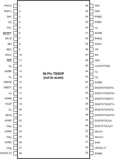
LM98722 30099502.gif

Pin Descriptions(1)

PIN I/O TYP RES DESCRIPTION
NO. NAME
1 PHIC2 O D PU Configurable high speed sensor timing output.
2 PHIC1 O D PD Configurable high speed sensor timing output.
3 SH1 O D PU Configurable low speed sensor timing output.
4 CE I D Chip Serial Interface Address Setting Input
CE LEVEL ADDRESS
VD 01
Float 10
DGND 00
5 CAL I D PD Initiate calibration sequence. Leave unconnected or tie to DGND if unused.
6 RESET I D PU Active-low master reset. NC when function not being used.
7 SH_R I D PD External request for an SH interval.
8 SDI I D PD Serial Interface Data Input.
9 SDO O D Serial Interface Data Output.
10 SCLK I D PD Serial Interface shift register clock.
11 SEN I D PU Active-low chip enable for the Serial Interface.
12 VA P Analog power supply. Bypass voltage source with 4.7μF and pin with 0.1μF to AGND.
13 AGND P Analog ground return.
14 VA P Analog power supply. Bypass voltage source with 4.7μF and pin with 0.1μF to AGND.
15 VREFB O A Bottom of ADC reference. Bypass with a 0.1μF capacitor to ground.
16 VREFT O A Top of ADC reference. Bypass with a 0.1μF capacitor to ground.
17 VA P Analog power supply. Bypass voltage source with 4.7μF and pin with 0.1μF to AGND.
18 AGND P Analog ground return.
19 VCLP IO A Input Clamp Voltage. Normally bypassed with a 0.1μF , and a 4.7μF capacitor to AGND. An external reference voltage may be applied to this pin.
20 VA P Analog power supply. Bypass voltage source with 4.7μF and pin with 0.1μF to AGND.
21 IBIAS O A Bias setting pin. Connect a 9.0 kΩ 1% resistor to AGND.
22 AGND P Analog ground return.
23 OSR I A Analog input signal. Typically sensor Red output AC-coupled thru a capacitor.
24 AGND P Analog ground return.
25 OSG I A Analog input signal. Typically sensor Green output AC-coupled thru a capacitor.
26 AGND P Analog ground return.
27 OSB I A Analog input signal. Typically sensor Blue output AC-coupled thru a capacitor.
28 CPOFILT2 A Charge Pump Filter Capacitor. Bypass this supply pin with a 0.1μF capacitor to CPOFILT1.
29 DGND P Digital ground return.
30 CPOFILT1 A Charge Pump Filter Capacitor. Bypass this supply pin with a 0.1μF capacitor to CPOFILT2.
31 DVB O D Digital Core Voltage bypass. Not an input. Bypass with 0.1μF capacitor to DGND.
32 INCLK+ I D Clock Input. Non-Inverting input for LVDS clocks or CMOS clock input. CMOS clock is selected when pin 33 is held at DGND, otherwise clock is configured for LVDS operation.
33 INCLK- I D Clock Input. Inverting input for LVDS clocks, connect to DGND for CMOS clock.
34 DOUT7/ O D Bit 7 of the digital video output bus in CMOS Mode, LVDS Frame Clock+ in LVDS Mode.
TXCLK+
35 DOUT6/ O D Bit 6 of the digital video output bus in CMOS Mode, LVDS Frame Clock- in LVDS Mode.
TXCLK-
36 DOUT5/ O D Bit 5 of the digital video output bus in CMOS Mode, LVDS Data Out2+ in LVDS Mode.
TXOUT2+
37 DOUT4/ O D Bit 4 of the digital video output bus in CMOS Mode, LVDS Data Out2- in LVDS Mode.
TXOUT2-
38 DOUT3/ O D Bit 3 of the digital video output bus in CMOS Mode, LVDS Data Out1+ in LVDS Mode.
TXOUT1+
39 DOUT2/ O D Bit 2 of the digital video output bus in CMOS Mode, LVDS Data Out1- in LVDS Mode.
TXOUT1-
40 DOUT1/ O D Bit 1 of the digital video output bus in CMOS Mode, LVDS Data Out0+ in LVDS Mode.
TXOUT0+
41 DOUT0/ O D Bit 0 of the digital video output bus in CMOS Mode, LVDS Data Out0- in LVDS Mode.
TXOUT0-
42 DGND O D PD Configurable sensor control output.
43 VD P Power supply for the digital circuits. Bypass this supply pin with 0.1μF capacitor. A single 4.7μF capacitor should be used between the supply and the VD, VR and VC pins.
44 VC P Power supply for the sensor control outputs. Bypass this supply pin with 0.1μF capacitor.
45 CLKOUT/SH2 O D Output clock for registering output data when using CMOS outputs, or a configurable low speed sensor timing output.
46 SH3 O D Configurable low speed sensor timing output.
47 RS O D Configurable high speed sensor timing output.
48 CP O D Configurable high speed sensor timing output.
49 PHIA1 O D Configurable high speed sensor timing output.
50 PHIA2 O D Configurable high speed sensor timing output.
51 DGND P Digital ground return.
52 VC P Power supply for the sensor control outputs.
Bypass this supply pin with 0.1μF capacitor.
53 PHIB1 O D Configurable high speed sensor timing output.
54 PHIB2 O D Configurable high speed sensor timing output.
55 SH4 O D Configurable low speed sensor timing output.
56 SH5 O D Configurable low speed sensor timing output.
(1) (I=Input), (O=Output), (IO=Bi-directional), (P=Power), (D=Digital), (A=Analog), (PU=Pull Up with an internal resistor), (PD=Pull Down with an internal resistor.).