SNAS558N January 2000 – March 2024 LMC555
PRODUCTION DATA
- 1
- 1 Features
- 2 Applications
- 3 Description
- 4 Pin Configuration and Functions
- 5 Specifications
- 6 Parameter Measurement Information
- 7 Detailed Description
- 8 Application and Implementation
- 9 Device and Documentation Support
- 10Revision History
- 11Mechanical, Packaging, and Orderable Information
Package Options
Refer to the PDF data sheet for device specific package drawings
Mechanical Data (Package|Pins)
- D|8
- P|8
- YPB|8
- DGK|8
Thermal pad, mechanical data (Package|Pins)
Orderable Information
7.4.1 Monostable Operation
In this mode of operation, the timer functions as a one-shot (Figure 7-2). The external capacitor is initially held discharged by internal circuitry. Upon application of a negative trigger pulse of less than 1/3 VS to the TRIGGER pin, the flip-flop is set, which both releases the short circuit across the capacitor and drives the output high.
 Figure 7-2 Monostable (One-Shot)
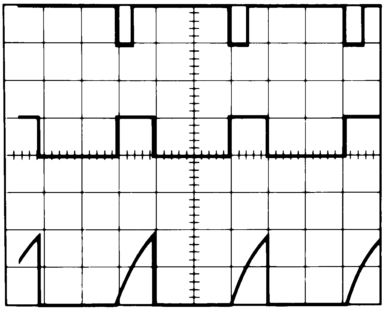
The voltage across the capacitor then increases exponentially for a period of tH = 1.1 RAC. This period is also the time that the output stays high, at the end of which time the voltage equals 2/3 VS. The comparator then resets the flip-flop, which in turn discharges the capacitor and drives the output to the low state. Figure 7-3 shows the waveforms generated in this mode of operation. Because the charge and the threshold level of the comparator are both directly proportional to supply voltage, the timing internal is independent of supply.

| VS = 5 V | Top trace: Input 5 V/div | RA = 9.1 kΩ |
| TIME = 0.1 ms/div | Middle trace: Output 5 V/div | C = 0.01 µF |
| Bottom trace: Capacitor voltage 2 V/div |
RESET overrides TRIGGER, which can override THRESHOLD. Therefore, ensure that the trigger pulse is shorter than the desired tH. The minimum pulse duration for TRIGGER is 20 ns, and is 400 ns for RESET. During the timing cycle when the output is high, the further application of a trigger pulse does not effect the circuit as long as the trigger input is returned high at least 10 µs before the end of the timing interval. However the circuit can be reset during this time by the application of a negative pulse to the RESET pin. The output remains in the low state until a trigger pulse is applied again.
When the reset function is not used, connect the RESET pin to V+ to avoid any possibility of false triggering. Figure 7-4 is a nomograph for easy determination of RC values for various time delays.
In monostable operation, drive the trigger high before the end of timing cycle.
 Figure 7-4 Time Delay