SNOS694I March 1995 – September 2015 LMC6001
PRODUCTION DATA.
- 1 Features
- 2 Applications
- 3 Description
- 4 Revision History
- 5 Pin Configuration and Functions
-
6 Specifications
- 6.1 Absolute Maximum Ratings
- 6.2 ESD Ratings
- 6.3 Recommended Operating Conditions
- 6.4 Thermal Information
- 6.5 DC Electrical Characteristics for LMC6001AI
- 6.6 DC Electrical Characteristics for LMC6001BI
- 6.7 DC Electrical Characteristics for LMC6001CI
- 6.8 AC Electrical Characteristics for LMC6001AIC
- 6.9 AC Electrical Characteristics for LM6001BI
- 6.10 AC Electrical Characteristics for LMC6001CI
- 6.11 Dissipation Ratings
- 6.12 Typical Characteristics
- 7 Detailed Description
- 8 Applications and Implementation
- 9 Power Supply Recommendations
- 10Layout
- 11Device and Documentation Support
- 12Mechanical, Packaging, and Orderable Information
Package Options
Mechanical Data (Package|Pins)
- P|8
Thermal pad, mechanical data (Package|Pins)
Orderable Information
8 Applications and Implementation
NOTE
Information in the following applications sections is not part of the TI component specification, and TI does not warrant its accuracy or completeness. TI’s customers are responsible for determining suitability of components for their purposes. Customers should validate and test their design implementation to confirm system functionality.
8.1 Application Information
8.1.1 Compensating For Input Capacitance
It is quite common to use large values of feedback resistance for amplifiers with ultra-low input current, like the LMC6001.
Although the LMC6001 is highly stable over a wide range of operating conditions, certain precautions must be met to achieve the desired pulse response when a large feedback resistor is used. Large feedback resistors with even small values of input capacitance, due to transducers, photodiodes, and printed-circuit-board parasitics, reduce phase margins.
When high input impedances are demanded, TI suggests guarding the LMC6001. Guarding input lines will not only reduce leakage, but lowers stray input capacitance as well. See Printed-Circuit-Board Layout For High-Impedance Work.
The effect of input capacitance can be compensated for by adding a capacitor, Cf, around the feedback resistors (as in Figure 19) such that:

or
Because it is often difficult to know the exact value of CIN, Cf can be experimentally adjusted so that the desired pulse response is achieved. Refer to the LMC660 (SNOSBZ3) and LMC662 (SNOSC51) for a more detailed discussion on compensating for input capacitance.
 Figure 19. Cancelling the Effect of Input Capacitance
8.1.2 Capacitive Load Tolerance
All rail-to-rail output swing operational amplifiers have voltage gain in the output stage. A compensation capacitor is normally included in this integrator stage. The frequency location of the dominant pole is affected by the resistive load on the amplifier. Capacitive load driving capability can be optimized by using an appropriate resistive load in parallel with the capacitive load. See Typical Characteristics.
Direct capacitive loading will reduce the phase margin of many op amps. A pole in the feedback loop is created by the combination of the output impedance of the op amp and the capacitive load. This pole induces phase lag at the unity-gain crossover frequency of the amplifier resulting in either an oscillatory or underdamped pulse response. With a few external components, op amps can easily indirectly drive capacitive loads, as shown in Figure 20.
 Figure 20. LMC6001 Noninverting Gain of 10 Amplifier, Compensated to Handle Capacitive Loads
In the circuit of Figure 20, R1 and C1 serve to counteract the loss of phase margin by feeding the high frequency component of the output signal back to the inverting input of the amplifier, thereby preserving phase margin in the overall feedback loop.
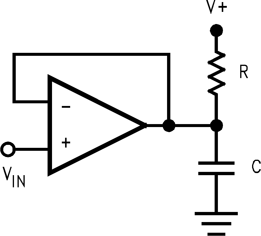
Capacitive load driving capability is enhanced by using a pullup resistor to V+ (Figure 21). Typically a pullup resistor conducting 500 μA or more will significantly improve capacitive load responses. The value of the pullup resistor must be determined based on the current sinking capability of the amplifier with respect to the desired output swing. Open-loop gain of the amplifier can also be affected by the pullup resistor. See DC Electrical Characteristics for LMC6001AI.
 Figure 21. Compensating for Large Capacitive Loads With a Pullup Resistor
8.2 Typical Application
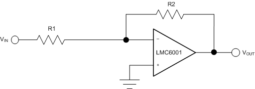
The extremely high input resistance, and low power consumption, of the LMC6001 make it ideal for applications that require battery-powered instrumentation amplifiers. Examples of these types of applications are hand-held pH probes, analytic medical instruments, electrostatic field detectors and gas chromotographs.
 Figure 22. Typical Application Schematic, LMC6001
8.2.1 Two Op Amp, Temperature Compensated Ph Probe Amplifier
The signal from a pH probe has a typical resistance between 10 MΩ and 1000 MΩ. Because of this high value, it is very important that the amplifier input currents be as small as possible. The LMC6001 with less than 25-fA input current is an ideal choice for this application.
The LMC6001 amplifies the probe output providing a scaled voltage of ±100 mV/pH from a pH of 7. The second op amp, a micropower LMC6041 provides phase inversion and offset so that the output is directly proportional to pH, over the full range of the probe. The pH reading can now be directly displayed on a low-cost, low-power digital panel meter. Total current consumption will be about 1 mA for the whole system.
The micropower dual-operational amplifier, LMC6042, would optimize power consumption but not offer these advantages:
- The LMC6001A ensures a 25-fA limit on input current at 25°C.
- The input ESD protection diodes in the LMC6042 are only rated at 500 V while the LMC6001 has much more robust protection that is rated at 2000 V.

| R1 100 k + 3500 ppm/°C | ||
| R2 68.1 k | ||
| R3, 8 5 k | ||
| R4, 9 100 k | ||
| R5 36.5 k | ||
| R6 619 k | ||
| R7 97.6 k | ||
| D1 LM4040D1Z-2.5 | ||
| C1 2.2 μF |
8.2.1.1 Design Requirements
The theoretical output of the standard Ag/AgCl pH probe is 59.16 mV/pH at 25°C with 0 V out at a pH of 7.00. This output is proportional to absolute temperature. To compensate for this, a temperature-compensating resistor, R1, is placed in the feedback loop. This cancels the temperature dependence of the probe. This resistor must be mounted where it will be at the same temperature as the liquid being measured.
8.2.1.2 Detailed Design Procedure
The set-up and calibration is simple with no interactions to cause problems.
- Disconnect the pH probe and with R3 set to about mid-range and the noninverting input of the LMC6001 grounded, adjust R8 until the output is 700 mV.
- Apply −414.1 mV to the noninverting input of the LMC6001. Adjust R3 for and output of 1400 mV. This completes the calibration. As real pH probes may not perform exactly to theory, minor gain and offset adjustments should be made by trimming while measuring a precision buffer solution.
8.2.1.3 Application Curve

| VS = ±5 V |
8.3 System Example
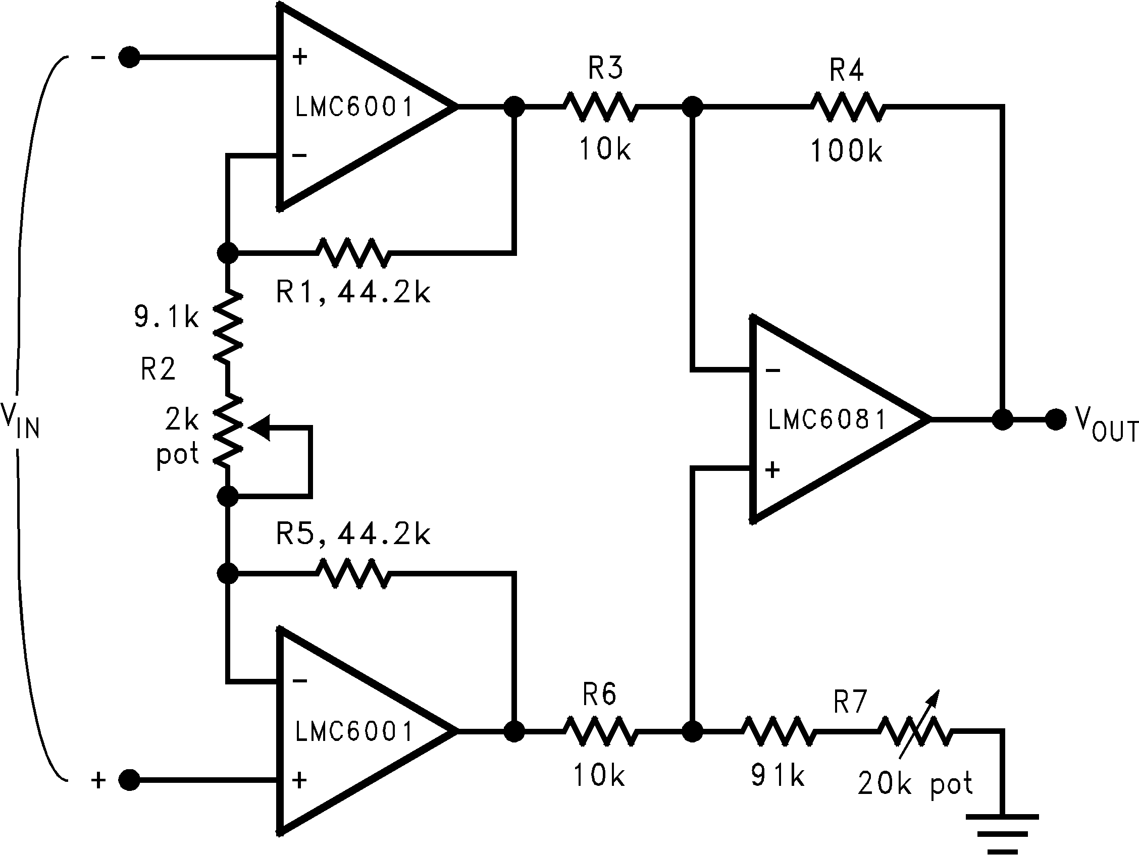
8.3.1 Ultra-Low Input Current Instrumentation Amplifier
Figure 25 shows an instrumentation amplifier that features high-differential and common-mode input resistance (>1014Ω), 0.01% gain accuracy at AV = 1000, excellent CMRR with 1-MΩ imbalance in source resistance. Input current is less than 20 fA and offset drift is less than 2.5 μV/°C. R2 provides a simple means of adjusting gain over a wide range without degrading CMRR. R7 is an initial trim used to maximize CMRR without using super precision matched resistors. For good CMRR over temperature, low-drift resistors should be used.

