SNOS609D November 1994 – February 2024 LMC6032 , LMC6034
PRODUCTION DATA
- 1
- 1Features
- 2Applications
- 3Description
- 4Pin Configuration and Functions
- 5Specifications
- 6Application and Implementation
- 7Device and Documentation Support
- 8Revision History
- 9Mechanical, Packaging, and Orderable Information
Package Options
Refer to the PDF data sheet for device specific package drawings
Mechanical Data (Package|Pins)
- D|8
- P|8
Thermal pad, mechanical data (Package|Pins)
Orderable Information
6.1.3 Capacitive Load Tolerance
Like many other op amps, the LMC603x can oscillate when applied a load that appears capacitive. The threshold of oscillation varies both with load and circuit gain. The configuration most sensitive to oscillation is a unity-gain follower. See also Section 5.7.
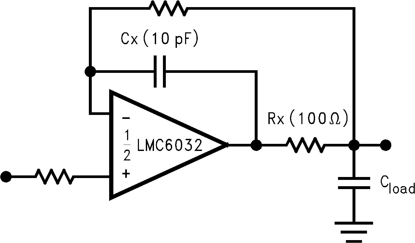
The load capacitance interacts with the op amp output resistance to create an additional pole. If this pole frequency is sufficiently low, the op amp phase margin is degraded so that the amplifier is no longer stable at low gains. Figure 6-3 shows that the addition of a small resistor (50Ω to 100Ω) in series with the op amp output, and a capacitor (5pF to 10pF) from inverting input to output pins, returns the phase margin to a safe value without interfering with lower-frequency circuit operation. Thus, larger values of capacitance can be tolerated without oscillation. In all cases, the output can ring heavily when the load capacitance is near the threshold for oscillation.
 Figure 6-3 Rx, Cx Improve Capacitive Load Tolerance
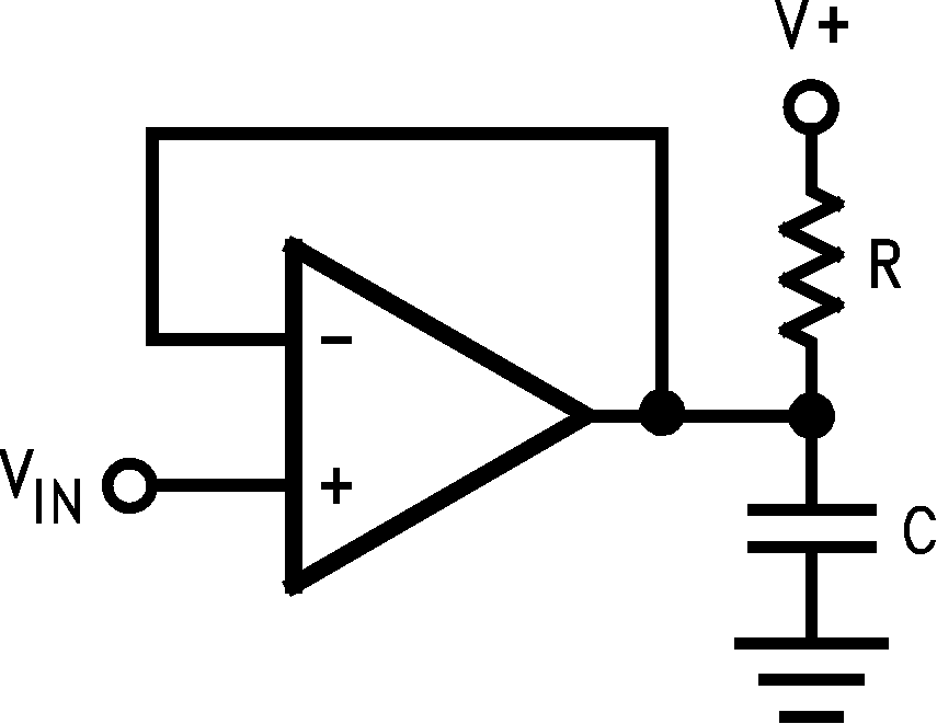
Capacitive load driving capability is enhanced by using a pullup resistor to V+ (Figure 6-4). Typically, a pullup resistor conducting 500μA or more significantly improves capacitive load responses. The value of the pullup resistor must be determined based on the current sinking capability of the amplifier with respect to the desired output swing. The open-loop gain of the amplifier can also be affected by the pullup resistor (see Section 5.6).
 Figure 6-4 Compensating for Large Capacitive Loads with a
Pullup Resistor