SNOS630E August 2000 – February 2024 LMC6081 , LMC6082 , LMC6084
PRODUCTION DATA
- 1
- 1Features
- 2Applications
- 3Description
- 4Pin Configuration and Functions
- 5Specifications
- 6Application and Implementation
- 7Device and Documentation Support
- 8Revision History
- 9Mechanical, Packaging, and Orderable Information
Package Options
Refer to the PDF data sheet for device specific package drawings
Mechanical Data (Package|Pins)
- D|14
Thermal pad, mechanical data (Package|Pins)
Orderable Information
6.3.1.1 Printed Circuit Board Layout for High-Impedance Work
Generally, any circuit that operates with less than 1000pA of leakage current requires special layout of the printed circuit board (PCB). To take advantage of the ultra-low bias current of the LMC608x, typically less than 10fA, an excellent layout is crucial. Fortunately, the techniques of obtaining low leakages are quite simple. First, do not ignore the surface leakage of the PCB, even though the leakage can sometimes appear acceptably low, because under conditions of high humidity or dust or contamination, the surface leakage can be appreciable.
To minimize the effect of any surface leakage, lay out a ring of foil completely surrounding the LMC608x inputs and the terminals of capacitors, diodes, conductors, resistors, relay terminals, and so on, connected to the op amp inputs, as in Figure 6-8. To have a significant effect, place guard rings on both the top and bottom of the PCB. This PCB foil must then be connected to a voltage that is at the same voltage as the amplifier inputs because no leakage current can flow between two points at the same potential. For example, a PCB trace-to-pad resistance of 1012Ω, which is normally considered a very large resistance, can leak 5pA if the trace were a 5V bus adjacent to the pad of the input. This leakage causes a 100 times degradation from the LMC608x actual performance. However, if a guard ring is held within 5mV of the inputs, then even a resistance of 1011Ω causes only 0.05pA of leakage current. See Figure 6-9 to Figure 6-11 for typical connections of guard rings for standard op amp configurations.
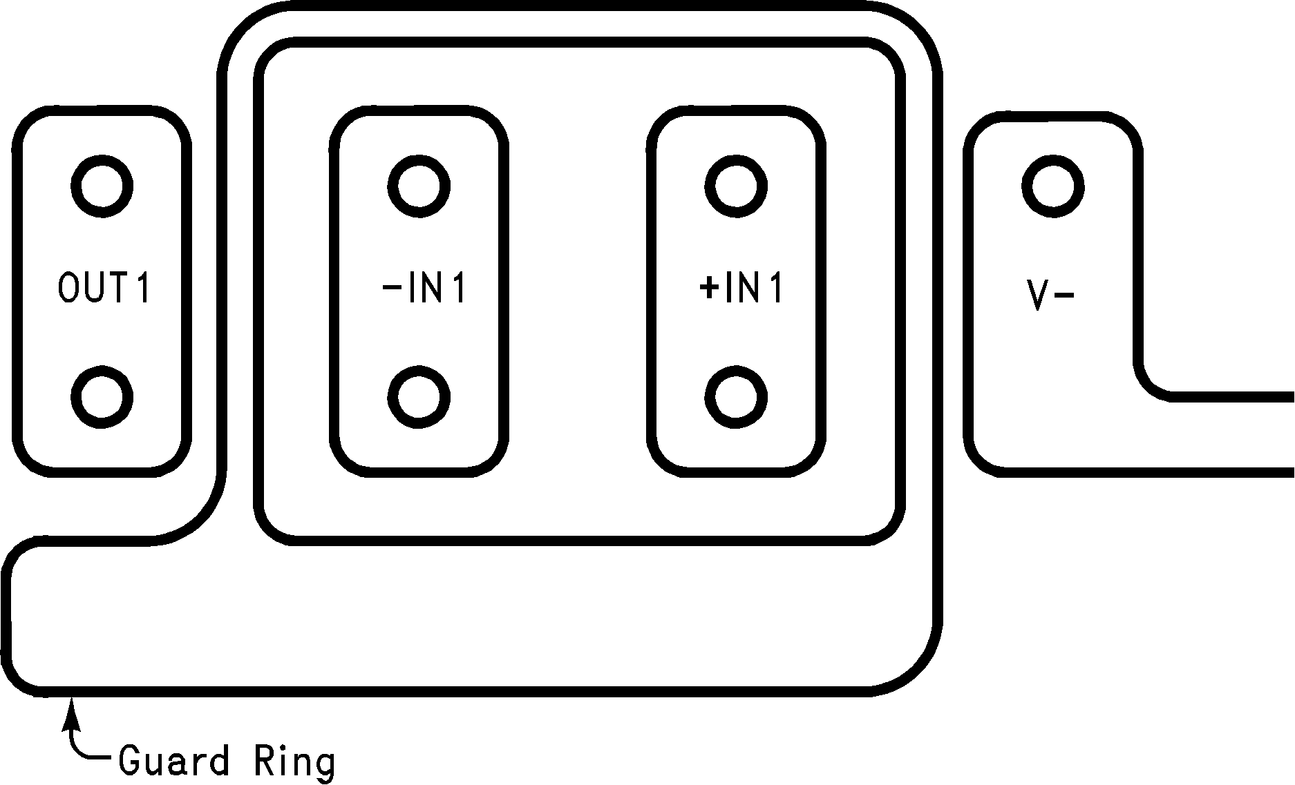 Figure 6-8 Example of Guard Ring in Printed Circuit Board
Layout
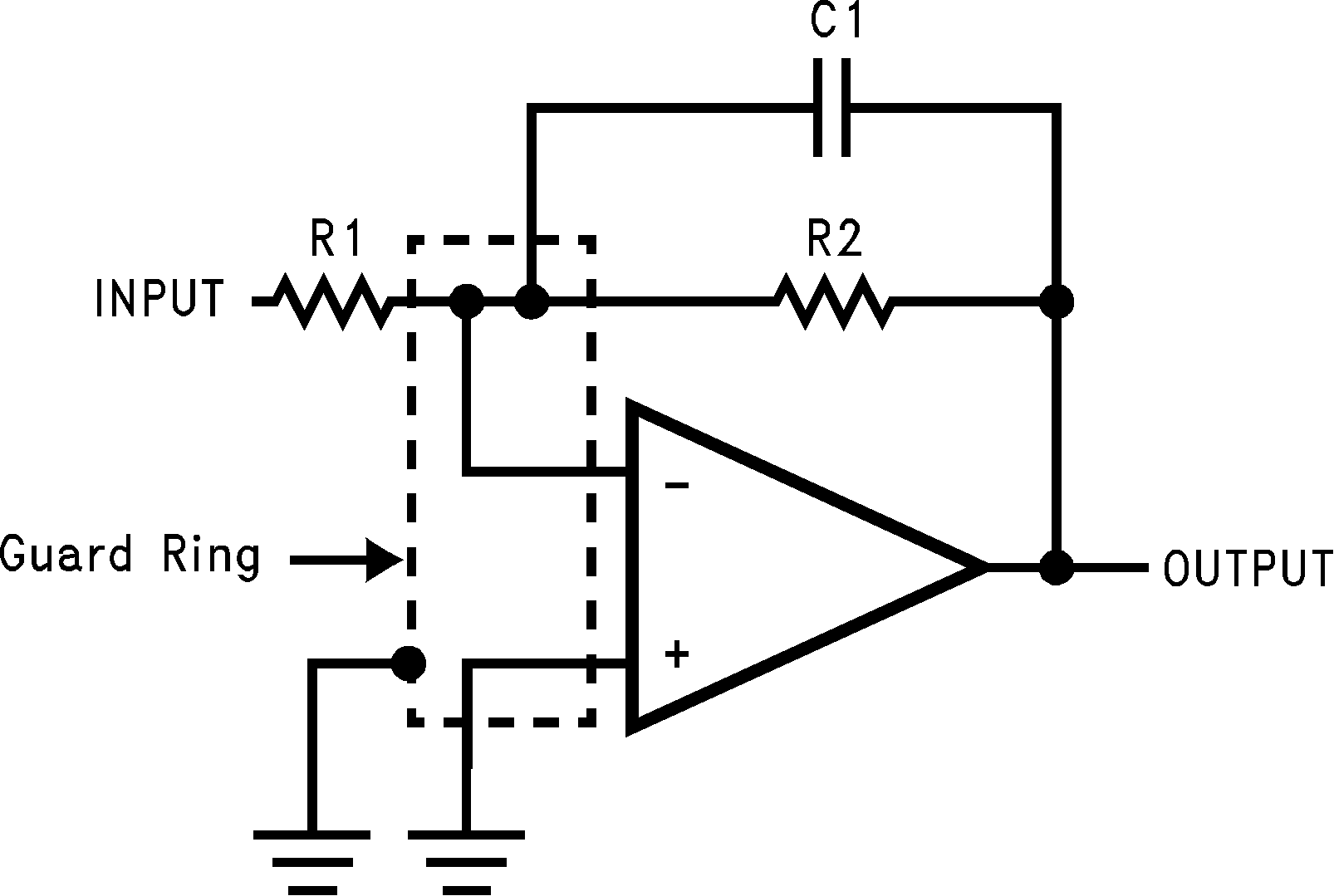 Figure 6-9 Typical Connections of Guard Rings:
Inverting Amplifier
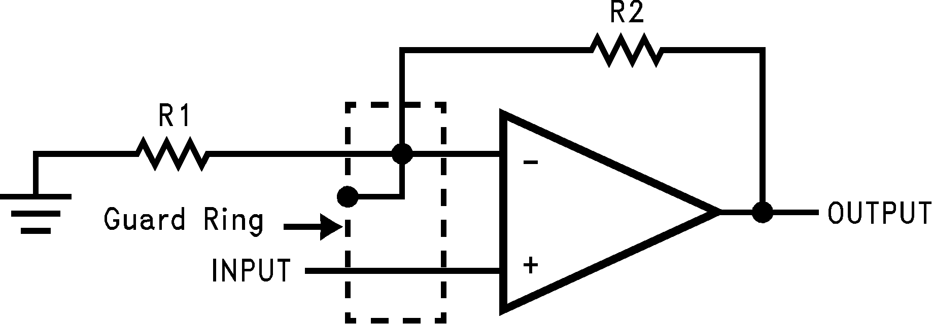 Figure 6-10 Typical Connections of Guard Rings:
Noninverting Amplifier
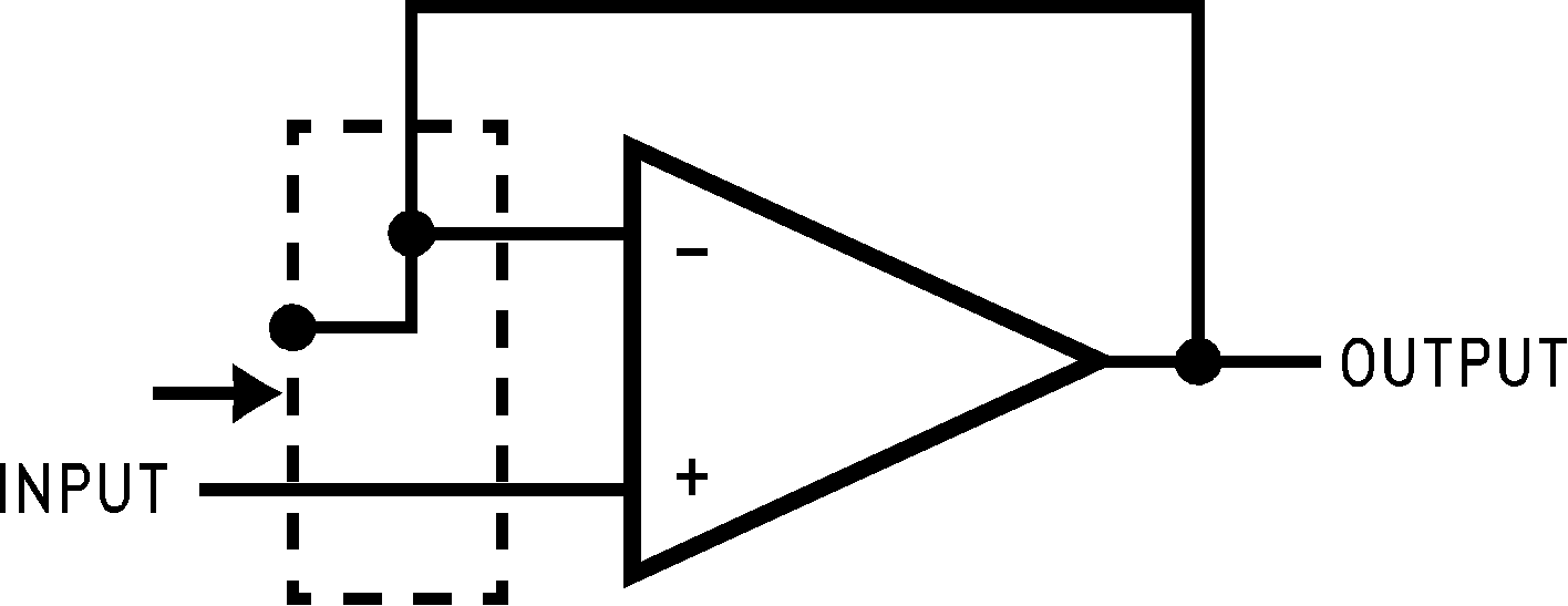 Figure 6-11 Typical Connections of Guard Rings:
Follower
Figure 6-11 Typical Connections of Guard Rings:
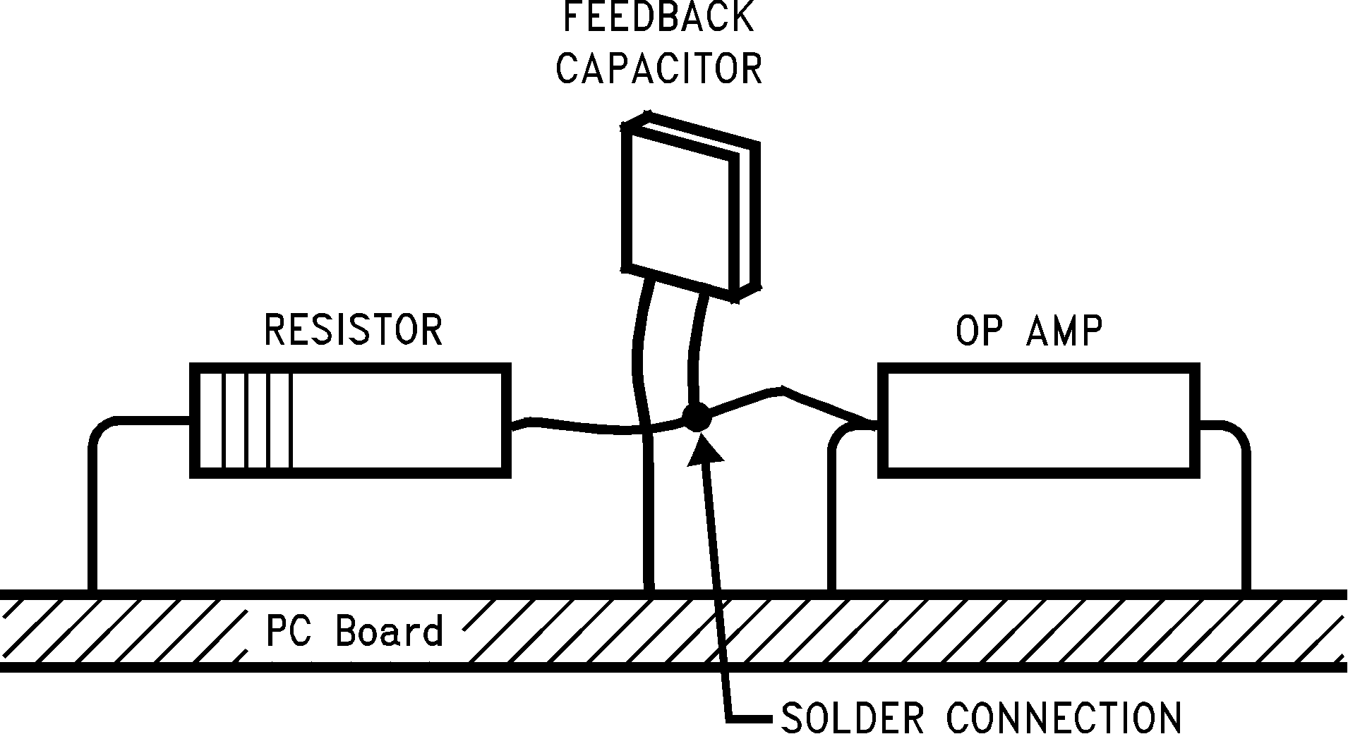
FollowerBe aware that when laying out a PCB for the sake of just a few circuits is inappropriate, there is another technique that is even better than a guard ring on a PCB. Do not insert the amplifier input pin into the board at all; instead, bend the pin up in the air and use only air as an insulator because air is an excellent insulator. In this case, some of the advantages of PCB construction are lost, but the advantages of air are sometimes well worth the effort of using point-to-point up-in-the-air wiring. See Figure 6-12.
