SNOS630E August 2000 – February 2024 LMC6081 , LMC6082 , LMC6084
PRODUCTION DATA
- 1
- 1Features
- 2Applications
- 3Description
- 4Pin Configuration and Functions
- 5Specifications
- 6Application and Implementation
- 7Device and Documentation Support
- 8Revision History
- 9Mechanical, Packaging, and Orderable Information
Package Options
Refer to the PDF data sheet for device specific package drawings
Mechanical Data (Package|Pins)
- D|14
Thermal pad, mechanical data (Package|Pins)
Orderable Information
6.2.1 Typical Single-Supply Applications
The extremely high input impedance, and low power consumption, make the LMC608x an excellent choice for applications that require battery-powered operation. Examples of these types of applications are hand-held pH probes, analytic medical instruments, magnetic field detectors, gas detectors, and silicon based pressure transducers.
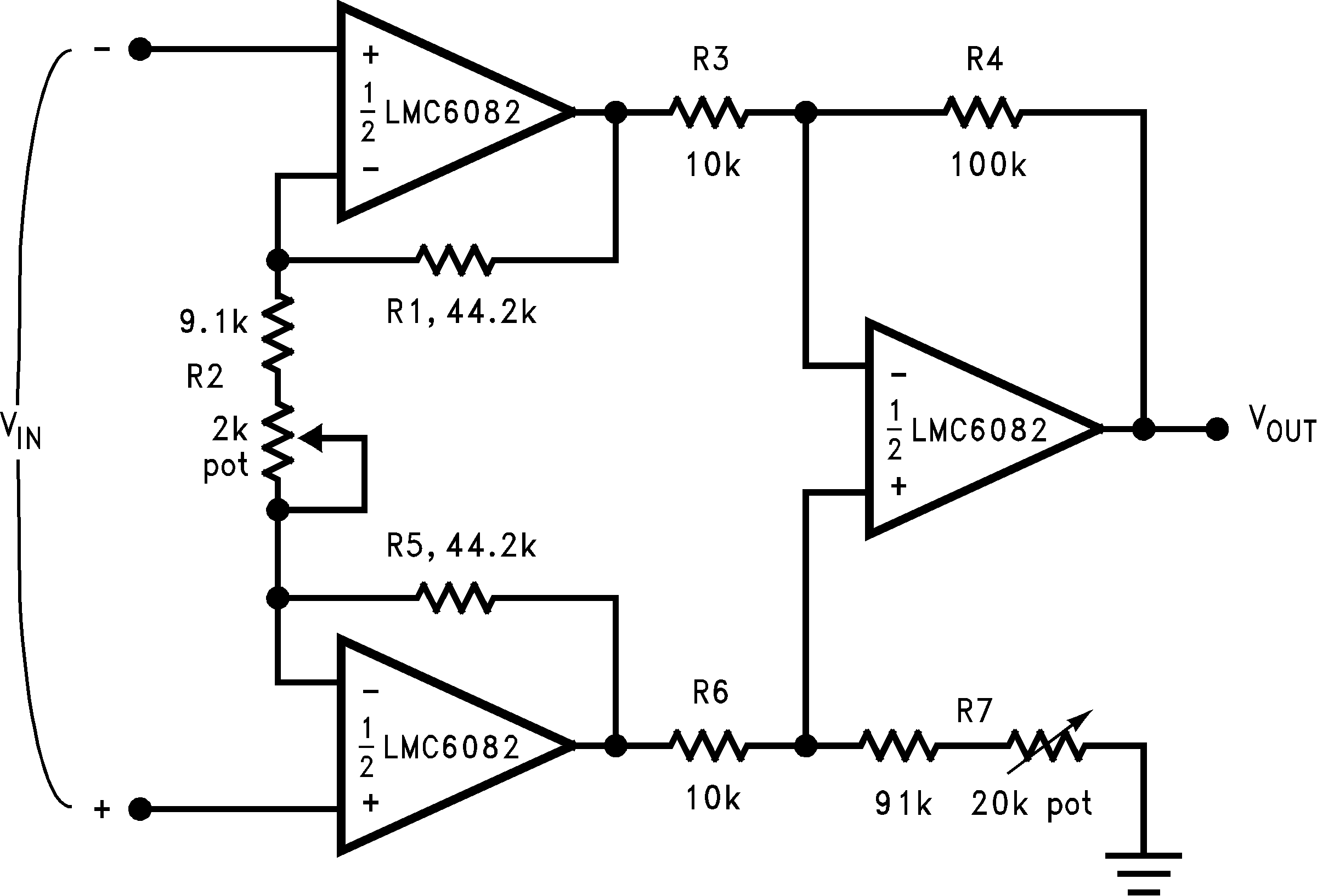
Figure 6-4 shows an instrumentation amplifier that features high differential and common mode input resistance (> 1014Ω), 0.01% gain accuracy at AV = 1000, excellent CMRR with 1kΩ imbalance in bridge source resistance. Input current is less than 100fA and offset drift is less than 2.5μV/°C. R2 provides a simple means of adjusting gain over a wide range without degrading CMRR. R7 is an initial trim used to maximize CMRR without using super precision matched resistors. For good CMRR over temperature, use low drift resistors like the RES11A. An example of an instrumentation amplifier with the LMC608x is provided in the next section.

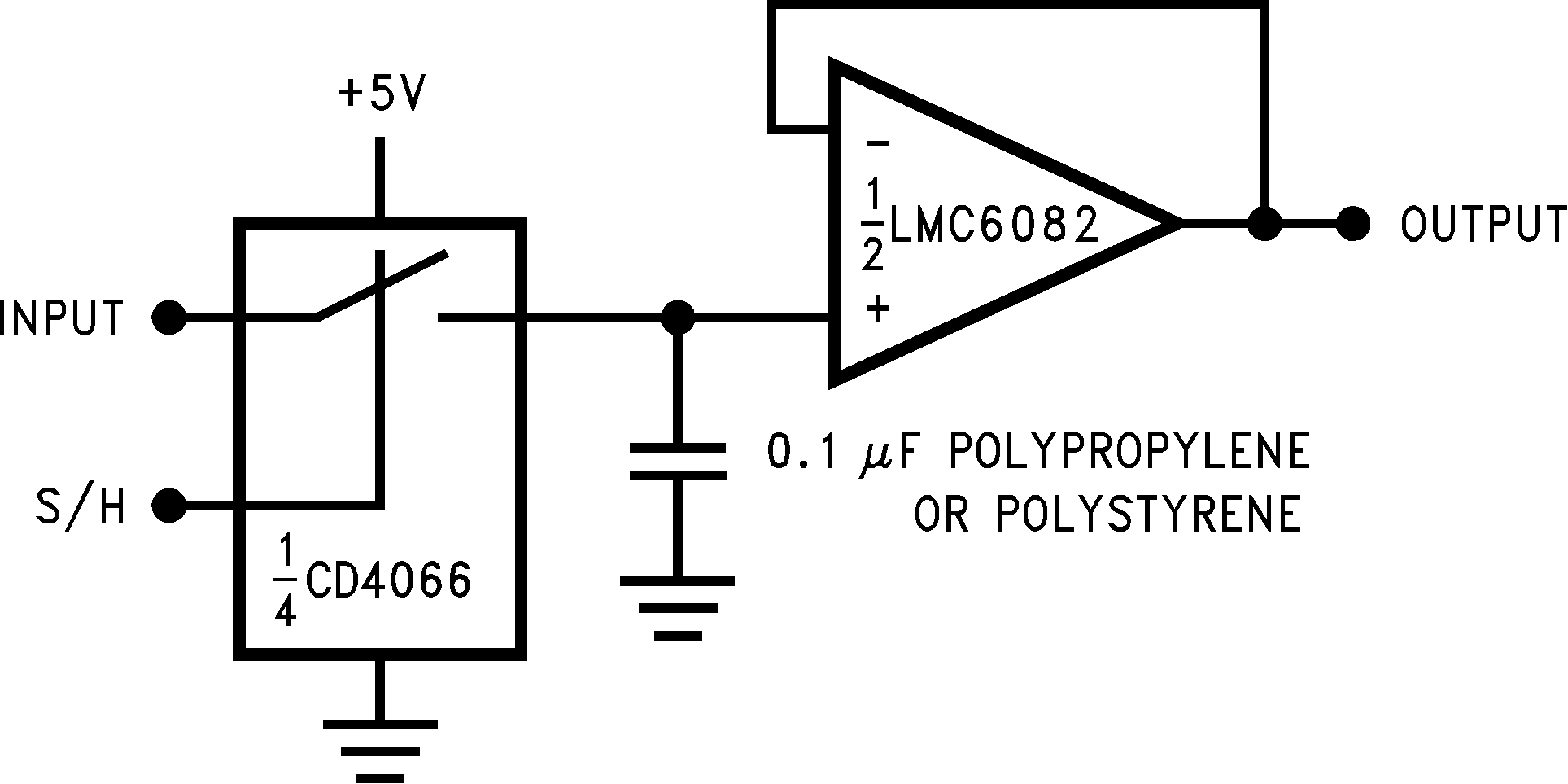
 Figure 6-5 Low Leakage Sample and
Hold
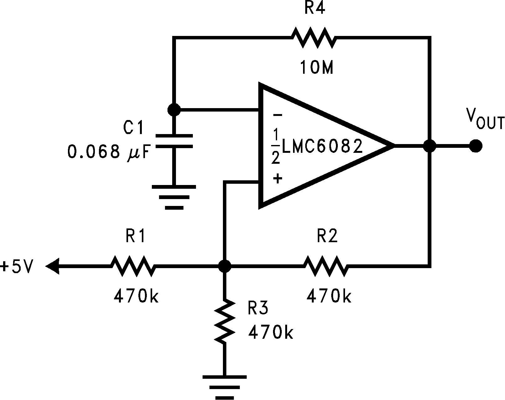
 Figure 6-6 1Hz Square-Wave
Oscillator