SNOS674J October   1997  – September 2024 LMC6482 , LMC6484

PRODUCTION DATA  

  1.   1
  2. Features
  3. Applications
  4. Description
  5. Pin Configuration and Functions
  6. Specifications
    1. 5.1 Absolute Maximum Ratings
    2. 5.2 ESD Ratings
    3. 5.3 Recommended Operating Conditions
    4. 5.4 Thermal Information LMC6482
    5. 5.5 Thermal Information LMC6484
    6. 5.6 Electrical Characteristics: VS = 5V
    7. 5.7 Electrical Characteristics: VS = 3V
    8. 5.8 Typical Characteristics
  7. Detailed Description
    1. 6.1 Overview
    2. 6.2 Functional Block Diagram
    3. 6.3 Feature Description
      1. 6.3.1 Amplifier Topology
      2. 6.3.2 Input Common-Mode Voltage Range
      3. 6.3.3 Rail-to-Rail Output
    4. 6.4 Device Functional Modes
  8. Application and Implementation
    1. 7.1 Application Information
      1. 7.1.1 Upgrading Applications
      2. 7.1.2 Data Acquisition Systems
      3. 7.1.3 Instrumentation Circuits
    2. 7.2 Typical Applications
      1. 7.2.1 3V Single-Supply Buffer Circuit
        1. 7.2.1.1 Design Requirements
        2. 7.2.1.2 Detailed Design Procedure
          1. 7.2.1.2.1 Capacitive Load Compensation
          2. 7.2.1.2.2 Capacitive Load Tolerance
          3. 7.2.1.2.3 Compensating For Input Capacitance
          4. 7.2.1.2.4 Offset Voltage Adjustment
        3. 7.2.1.3 Application Curves
      2. 7.2.2 Typical Single-Supply Applications
    3. 7.3 Power Supply Recommendations
    4. 7.4 Layout
      1. 7.4.1 Layout Guidelines
      2. 7.4.2 Layout Example
  9. Device and Documentation Support
    1. 8.1 Device Support
      1. 8.1.1 Development Support
        1. 8.1.1.1 Spice Macromodel
        2. 8.1.1.2 PSpice® for TI
        3. 8.1.1.3 TINA-TI™ Simulation Software (Free Download)
        4. 8.1.1.4 DIP-Adapter-EVM
        5. 8.1.1.5 DIYAMP-EVM
        6. 8.1.1.6 TI Reference Designs
        7. 8.1.1.7 Analog Filter Designer
    2. 8.2 Receiving Notification of Documentation Updates
    3. 8.3 Support Resources
    4. 8.4 Trademarks
    5. 8.5 Electrostatic Discharge Caution
    6. 8.6 Glossary
  10. Revision History
  11. 10Mechanical, Packaging, and Orderable Information

Package Options

Refer to the PDF data sheet for device specific package drawings

Mechanical Data (Package|Pins)
  • D|8
  • P|8
  • DGK|8
Thermal pad, mechanical data (Package|Pins)
Orderable Information

Input Common-Mode Voltage Range

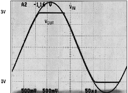
Unlike Bi-FET amplifier designs, the LMC648x do not exhibit phase inversion when an input voltage exceeds the negative supply voltage. Figure 6-2 shows an input voltage exceeding both supplies with no resulting phase inversion on the output.

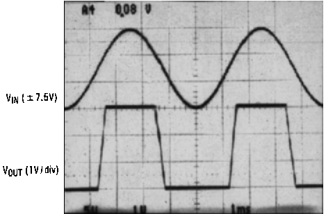
The absolute maximum input voltage is 300mV beyond either supply rail at room temperature. Voltages greatly exceeding this absolute maximum rating, as in Figure 6-3, can cause excessive current to flow in or out of the input pins possibly affecting reliability.
LMC6482  LMC6484 Input Voltage
An input voltage signal exceeds the LMC6482 power supply voltages with no output phase inversion.
Figure 6-2 Input Voltage
LMC6482  LMC6484 Input Signal
A ±7.5‑V input signal greatly exceeds the 3‑V supply in Figure 6-4 causing no phase inversion due to Ri.
Figure 6-3 Input Signal

Applications that exceed this rating must externally limit the maximum input current to ±5mA with an input resistor (Ri) as shown in Figure 6-4.

LMC6482  LMC6484 Ri Input Current
                    Protection for Voltages Exceeding the Supply Voltages
NOTE: Ri input current protection for voltages exceeding the supply voltages.
Figure 6-4 Ri Input Current Protection for Voltages Exceeding the Supply Voltages