SNOS674J October   1997  – September 2024 LMC6482 , LMC6484

PRODUCTION DATA  

  1.   1
  2. Features
  3. Applications
  4. Description
  5. Pin Configuration and Functions
  6. Specifications
    1. 5.1 Absolute Maximum Ratings
    2. 5.2 ESD Ratings
    3. 5.3 Recommended Operating Conditions
    4. 5.4 Thermal Information LMC6482
    5. 5.5 Thermal Information LMC6484
    6. 5.6 Electrical Characteristics: VS = 5V
    7. 5.7 Electrical Characteristics: VS = 3V
    8. 5.8 Typical Characteristics
  7. Detailed Description
    1. 6.1 Overview
    2. 6.2 Functional Block Diagram
    3. 6.3 Feature Description
      1. 6.3.1 Amplifier Topology
      2. 6.3.2 Input Common-Mode Voltage Range
      3. 6.3.3 Rail-to-Rail Output
    4. 6.4 Device Functional Modes
  8. Application and Implementation
    1. 7.1 Application Information
      1. 7.1.1 Upgrading Applications
      2. 7.1.2 Data Acquisition Systems
      3. 7.1.3 Instrumentation Circuits
    2. 7.2 Typical Applications
      1. 7.2.1 3V Single-Supply Buffer Circuit
        1. 7.2.1.1 Design Requirements
        2. 7.2.1.2 Detailed Design Procedure
          1. 7.2.1.2.1 Capacitive Load Compensation
          2. 7.2.1.2.2 Capacitive Load Tolerance
          3. 7.2.1.2.3 Compensating For Input Capacitance
          4. 7.2.1.2.4 Offset Voltage Adjustment
        3. 7.2.1.3 Application Curves
      2. 7.2.2 Typical Single-Supply Applications
    3. 7.3 Power Supply Recommendations
    4. 7.4 Layout
      1. 7.4.1 Layout Guidelines
      2. 7.4.2 Layout Example
  9. Device and Documentation Support
    1. 8.1 Device Support
      1. 8.1.1 Development Support
        1. 8.1.1.1 Spice Macromodel
        2. 8.1.1.2 PSpice® for TI
        3. 8.1.1.3 TINA-TI™ Simulation Software (Free Download)
        4. 8.1.1.4 DIP-Adapter-EVM
        5. 8.1.1.5 DIYAMP-EVM
        6. 8.1.1.6 TI Reference Designs
        7. 8.1.1.7 Analog Filter Designer
    2. 8.2 Receiving Notification of Documentation Updates
    3. 8.3 Support Resources
    4. 8.4 Trademarks
    5. 8.5 Electrostatic Discharge Caution
    6. 8.6 Glossary
  10. Revision History
  11. 10Mechanical, Packaging, and Orderable Information

Package Options

Refer to the PDF data sheet for device specific package drawings

Mechanical Data (Package|Pins)
  • D|14
  • N|14
Thermal pad, mechanical data (Package|Pins)
Orderable Information
Capacitive Load Compensation

The LMC648x provides a robust output stage for directly driving capacitive loads. Capacitive loads interact with the output impedance of the amplifier to create a pole that can cause instability. When driving capacitive loads, consider the closed-loop bandwidth and output impedance of the amplifier. The LMC648x open-loop output impedance is shown in Figure 7-7.

LMC6482  LMC6484 Open-Loop Output
                    Impedance Figure 7-7 Open-Loop Output Impedance

In some applications, driving large capacitive loads is required and additional compensation is necessary. Capacitive load compensation can be accomplished using resistive isolation as shown in Figure 7-8. This simple technique is useful for isolating the capacitive inputs of multiplexers and analog-to-digital converters (ADCs).

LMC6482  LMC6484 Resistive Isolation of a
                        330pF Capacitive LoadFigure 7-8 Resistive Isolation of a 330pF Capacitive Load
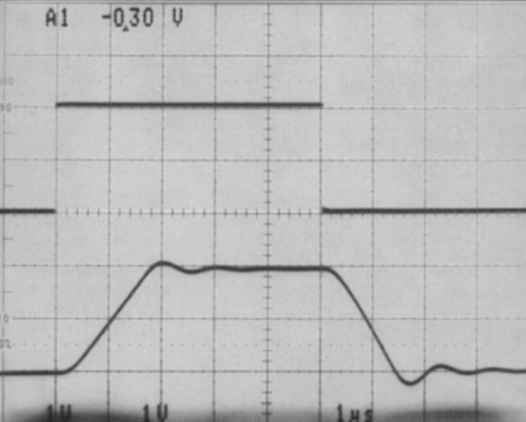
LMC6482  LMC6484 Pulse Response of the
                        LMC6482 Circuit in Figure 7-8Figure 7-9 Pulse Response of the LMC6482 Circuit in Figure 7-8