SNOS724F August 2000 – February 2024 LMC6492 , LMC6494
PRODUCTION DATA
- 1
- 1Features
- 2Applications
- 3Description
- 4Pin Configuration and Functions
- 5Specifications
- 6Application and Implementation
- 7Device and Documentation Support
- 8Revision History
- 9Mechanical, Packaging, and Orderable Information
Package Options
Refer to the PDF data sheet for device specific package drawings
Mechanical Data (Package|Pins)
- D|8
Thermal pad, mechanical data (Package|Pins)
Orderable Information
6.1.4 Capacitive Load Tolerance
All rail-to-rail output swing operational amplifiers have voltage gain in the output stage. A compensation capacitor is normally included in this integrator stage. The frequency location of the dominant pole is affected by the resistive load on the amplifier. Capacitive load driving capability can be optimized by using an appropriate resistive load in parallel with the capacitive load (see Typical Curves).
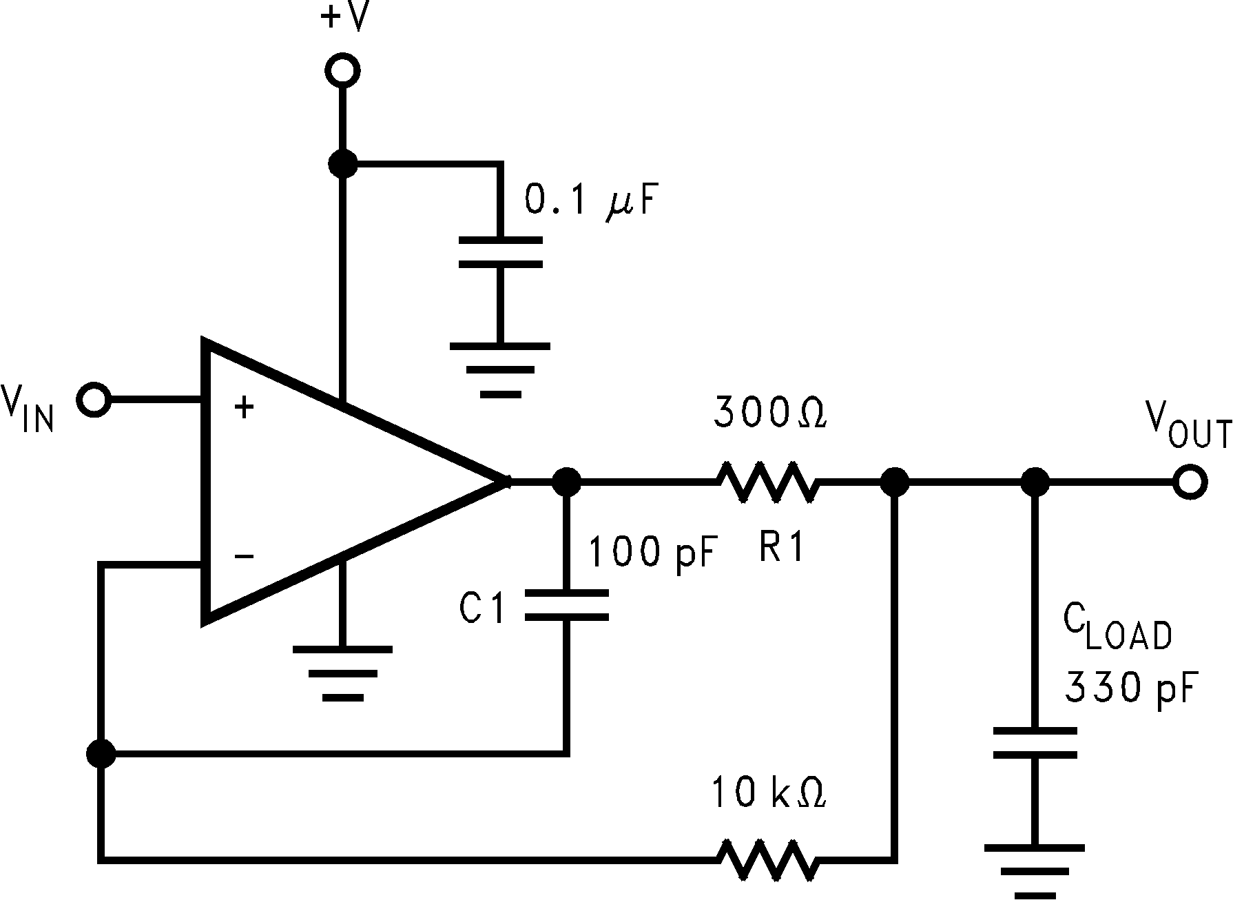
Direct capacitive loading reduces the phase margin of many op amps. A pole in the feedback loop is created by the combination of the op amp output impedance and the capacitive load. The open-loop output impedance of the LMC649x is shown in Figure 6-6. This pole induces phase lag at the unity-gain crossover frequency of the amplifier resulting in either an oscillatory or underdamped pulse response. With a few external components, op amps can easily indirectly drive capacitive loads, as shown in Figure 6-7.
 Figure 6-6 LMC649x Open-Loop Ouput Impedance
 Figure 6-7 LMC649x Noninverting Amplifier, Compensated to
Handle Capacitive Loads