SNOS724F August 2000 – February 2024 LMC6492 , LMC6494
PRODUCTION DATA
- 1
- 1Features
- 2Applications
- 3Description
- 4Pin Configuration and Functions
- 5Specifications
- 6Application and Implementation
- 7Device and Documentation Support
- 8Revision History
- 9Mechanical, Packaging, and Orderable Information
Package Options
Refer to the PDF data sheet for device specific package drawings
Mechanical Data (Package|Pins)
- D|8
Thermal pad, mechanical data (Package|Pins)
Orderable Information
6.1.1 Input Common-Mode Voltage Range
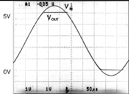
Unlike Bi-FET amplifier designs, the LMC649x does not exhibit phase inversion when an input voltage exceeds the negative supply voltage. Figure 6-1 shows an input voltage exceeding both supplies with no resulting phase inversion on the output.
 Figure 6-1 Input Voltage Signal Exceeds
the
Figure 6-1 Input Voltage Signal Exceeds
theLMC649x Power Supply Voltages With
No Output Phase Inversion
The LMC649x is a true rail-to-rail input operational amplifier with an input common-mode range that extends beyond either supply rail. When the input common-mode voltage swings to about 3V from the positive rail, some dc specifications, namely offset voltage, can be slightly degraded. Figure 6-2 illustrates the input offset behavior across the entire common-mode range.
 Figure 6-2 Input Offset Voltage vs Common-Mode Voltage
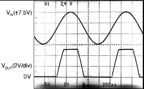
The absolute maximum input voltage is 300mV beyond either supply rail at room temperature. Voltages greatly exceeding this absolute maximum rating, as in Figure 6-3, can cause excessive current to flow in or out of the input pins possibly affecting reliability.
 Figure 6-3 A ±7.5V Input Signal Greatly
Exceeds the 5V Supply in Figure 6-3, Causing No Phase Inversion Due to
RI
Figure 6-3 A ±7.5V Input Signal Greatly
Exceeds the 5V Supply in Figure 6-3, Causing No Phase Inversion Due to
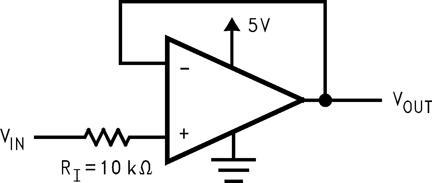
RIApplications that exceed this rating must externally limit the maximum input current to ±5mA with an input resistor (RI) as shown in Figure 6-4.
 Figure 6-4 RI Input Current Protection for
Voltages Exceeding the Supply Voltages