SNOS724F August 2000 – February 2024 LMC6492 , LMC6494
PRODUCTION DATA
- 1
- 1Features
- 2Applications
- 3Description
- 4Pin Configuration and Functions
- 5Specifications
- 6Application and Implementation
- 7Device and Documentation Support
- 8Revision History
- 9Mechanical, Packaging, and Orderable Information
Package Options
Refer to the PDF data sheet for device specific package drawings
Mechanical Data (Package|Pins)
- D|14
Thermal pad, mechanical data (Package|Pins)
- D|14
Orderable Information
6.2.1 Application Circuits

(V1 + V2 ≥ (V3 + V4) to keep V0 > 0VDC
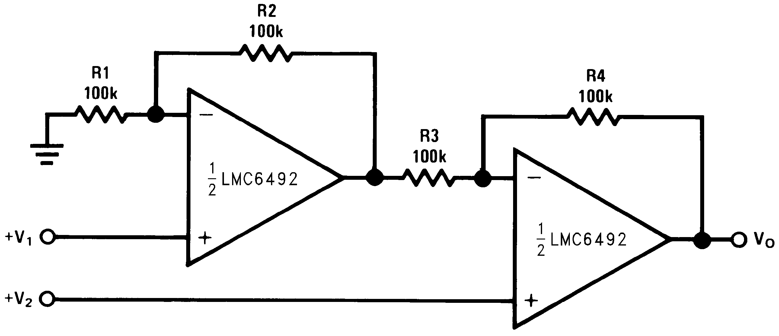
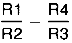

 Figure 6-10 Photo Voltaic-Cell Amplifier
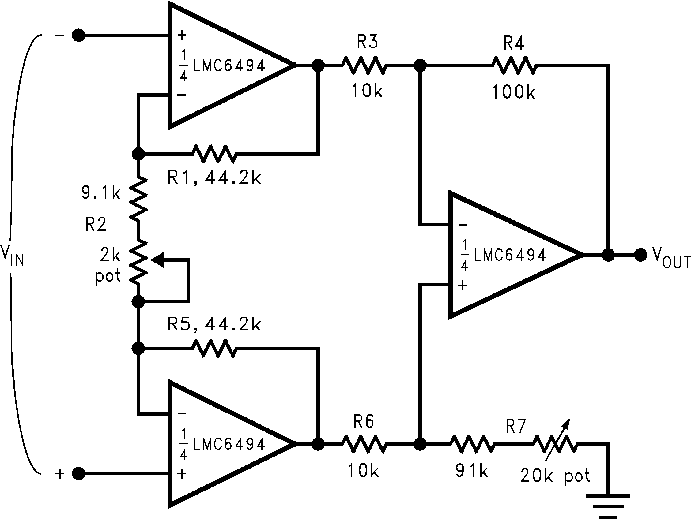

 Figure 6-12 Rail-to-Rail Single Supply Low Pass Filter
This low-pass filter circuit can be used as an antialiasing filter with the same supply as the ADC. Filter designs can also take advantage of the LMC649x ultra-low input current. The ultra-low input current yields negligible offset error even when large value resistors are used. This configuration in turn allows the use of smaller-valued capacitors that take up less board space and cost less.
 Figure 6-13 Low Voltage Peak Detector with Rail-to-Rail Peak Capture Range
Dielectric absorption and leakage is minimized by using a polystyrene or polypropylene hold capacitor. The droop rate is primarily determined by the value of CHOLD and diode leakage current. Select low-leakage current diodes to minimize drooping.
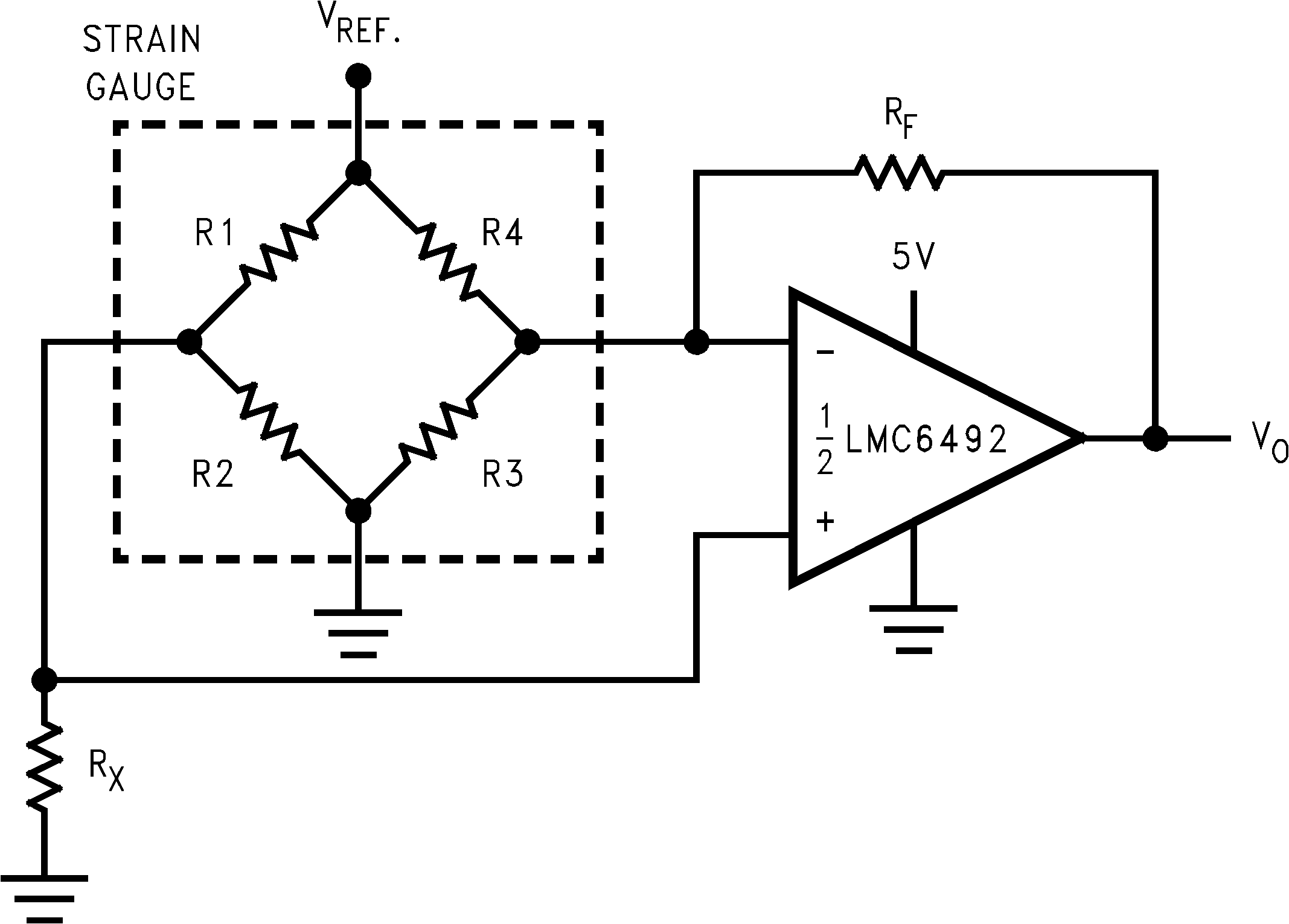
Rf >> R1, R2, R3, and R4
 Figure 6-14 Pressure Sensor
In a manifold absolute pressure sensor application, a strain gauge is mounted on the intake manifold in the engine unit. Manifold pressure causes the sensing resistors, R1, R2, R3 and R4 to change. The resistors change in a way such that R2 and R4 increase by the same amount R1 and R3 decrease. This causes a differential voltage between the input of the amplifier. The gain of the amplifier is adjusted by Rf.