SNOS724F August 2000 – February 2024 LMC6492 , LMC6494
PRODUCTION DATA
- 1
- 1Features
- 2Applications
- 3Description
- 4Pin Configuration and Functions
- 5Specifications
- 6Application and Implementation
- 7Device and Documentation Support
- 8Revision History
- 9Mechanical, Packaging, and Orderable Information
Package Options
Refer to the PDF data sheet for device specific package drawings
Mechanical Data (Package|Pins)
- D|14
Thermal pad, mechanical data (Package|Pins)
- D|14
Orderable Information
6.1.3 Compensating for Input Capacitance
Large values of feedback resistance are commonly used for amplifiers with ultra-low input current, such as the LMC649x.
Although the LMC649x is highly stable over a wide range of operating conditions, make sure that certain precautions are met to achieve the desired pulse response when a large feedback resistor is used. Large feedback resistors with even small values of input capacitance (due to transducers, photodiodes, and circuit board parasitics) reduce phase margins.
When high input impedances are demanded, guarding of the LMC649x is suggested. Guarding input lines not only reduces leakage, but also lowers stray input capacitance. See Printed-Circuit-Board Layout for High Impedance Work.
The effect of input capacitance can be compensated by adding a capacitor, Cf, around the feedback resistors (as in Figure 6-1 ) so that:
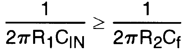
or
The exact value of CIN is difficult to know; therefore, Cf can be experimentally adjusted so that the desired pulse response is achieved. See the LMC660 and LMC662 for a more detailed discussion on compensating for input capacitance.
 Figure 6-5 Canceling the Effect of Input
Capacitance
Figure 6-5 Canceling the Effect of Input
Capacitance