SNOSD12D November 2018 – January 2019 LMG1210
PRODUCTION DATA.
- 1 Features
- 2 Applications
- 3 Description
- 4 Revision History
- 5 Pin Configuration and Functions
- 6 Specifications
- 7 Detailed Description
- 8 Application and Implementation
- 9 Power Supply Recommendations
- 10Layout
- 11Device and Documentation Support
- 12Mechanical, Packaging, and Orderable Information
Package Options
Mechanical Data (Package|Pins)
- RVR|19
Thermal pad, mechanical data (Package|Pins)
Orderable Information
7.4 Device Functional Modes
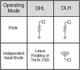
The mode of operation is determined by the state of DHL and DLH pins during power up. The state of the pins is sampled at power up and cannot be changed during operation. There are two different modes: independent operation where separate HI and LI signals are required, and PWM mode where one PWM input signal is required and the LMG1210 generates the complementary HI and LI signals. For PWM input, the dead time for the low-to-high and high-to-low switch-node transition is independently set by an external resistor at DHL and DLH. For independent input mode, DLH is tied to VDD and DHL is internally set to high-impedance and can be tied to VDD, tied to ground or left floating.
 Figure 16. Operation Mode Selection
 Table 1 lists the functional modes for the LMG1210.
Table 1. LMG1210 Truth Table
| INPUTS | PWM MODE | INDEPENDENT MODE | |||
|---|---|---|---|---|---|
| EN/HI | PWM/LI | HO | LO | HO | LO |
| 0 | 0 | 0 | 0 | 0 | 0 |
| 0 | 1 | 0 | 0 | 0 | 1 |
| 1 | 0 | 0 | 1 | 1 | 0 |
| 1 | 1 | 1 | 0 | 1 | 1 |